This thread has been locked.

If you have a related question, please click the "Ask a related question" button in the top right corner. The newly created question will be automatically linked to this question.

DS320PR810: Lane Configration

Part Number: DS320PR810

DS320PR810 Lane Configration question 

I make a board used two DS320PR810 .

I put singnal of PHY first then , Lane configration is blelow.

Host         DS320PR810(No1)    DS320PR810(No2)   

Lane1      Lane2                           Lane5

Lane2     Lane4                            Lane3

Lane3     Lane5                            Lane2

Lane4     Lane6                            Lane1


 Does your devices work?

 if your device doesn't work , does it work by modyfied show below?

Host         DS320PR810(No1)    DS320PR810(No2)   

Lane1      Lane3(change)                  Lane4(change)

Lane2     Lane4                                Lane3

Lane3     Lane5                                Lane2

Lane4     Lane6                               Lane1

  • Hello,

    I am not sure if I understand the meaning of your lane configuration tables. Do you have a block diagram of the organization of CPU <---> DS320PR810 redrivers <---> Endpoint (SSD?) and how the signals may be routed on this path?

    In general, the DS320PR810 and other linear redrivers are not protocol-aware devices. Lanes are a PCIe idea, they are organized and determined by the CPU as part of the PCIe protocol. This means that the device only sees and manages the status of the 8 channels when they are in the device, it does not know or care how the inputs or outputs may be linked as long as the correct directions are followed. For example, I could connect CPU TX7 --> redriver RX5, and then redriver TX5 --> SSD RX0, this would form an electrical connection between CPU TX7 and SSD RX0.

    Best,

    Evan Su

  • The lane configration that I say stand for pin name, below.

    *1st Redriver Configration

    Host     Redriver      Redriver   SSD

     Tx0     Rx2              Tx2           Rx0

     Tx1     Rx4              Tx4           Rx1

     Tx2     Rx5             Tx5            Rx2

     Tx3     Rx6             Tx6            Rx3

     Rx0    Tx2              Rx2           Tx0

     Rx1    Tx4              Rx4           Tx1

     Rx2    Tx5              Rx5           Tx2

     Rx3    Tx6              Rx6           Tx3

      +1st Rediriver have missing lane3.

    *2nd Rediver Configration

    Host     Redriver      Redriver   SSD

     Tx0     Rx5              Tx5           Rx0

     Tx1     Rx3              Tx3           Rx1

     Tx2     Rx2             Tx2            Rx2

     Tx3     Rx1             Tx1            Rx3

     Rx0    Tx5              Rx5           Tx0

     Rx1    Tx3              Rx3           Tx1

     Rx2    Tx2              Rx2           Tx2

     Rx3    Tx1              Rx1           Tx3

      +1st Rediriver have missing lane4.

     I think missing lane make no probrem under your comment,Please check it.

  • Hello,

    Thanks for the new information. I am confused because it looks like you are saying that each redriver has two directions of data (Host TX to SSD RX, SSD TX to Host RX). The DS320PR810 is a unidirectional device so all 8 channels are in one direction, it would be difficult to have two data directions in one device.

    Do you have a schematic for your board? If it is confidential, you can request friendship from my forum profile and send it to me in private messages for review, this way the organization would be more clear to me.

    Best,

    Evan Su

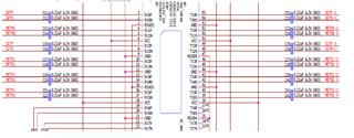
  • I simply use this IC. Input/output of redriver(No1) is above.(Can you see?)

    (RX2 in my repry means Rx1p/n in this figure.)

    S1Tp/n and  S0Tp/n are normaly unused. 

     This IC(No1) work Host TX->SSD RX.

     Another IC(No2) work SSD TX->Host RX.

    This is one direction usage,isn't it?

    Regard.

  • I notice typo in my reply.

    Lane confgiration was below,(I correct number of lanes too.)  

    +No1

    Host     Redriver(In)  Redriver(out)   SSD(in)

     Tx0     Rx1              Tx1                   Rx0

     Tx1     Rx3              Tx3                  Rx1

     Tx2     Rx4              Tx4                  Rx2

    Tx3      Rx5              Tx5                  Rx3

    +No2

    Host    Redriver(In)  Redriver(out)   SSD(Out)

     Rx0     Tx1              Rx1                 Tx0

     Rx1    Tx3              Rx3                 Tx1

     Rx2    Tx4              Rx4                 Tx2

     Rx3    Tx5              Rx5                 Tx3

  • Hello,

    Thanks for the clarification. From what I see in your schematic and new table, these connections should be OK.

    I have a small note after looking at the schematic:

    • If there are redriver TX/RX pins that are never used in any case, ideally they can be terminated to GND through 50 Ohm resistors in order to prevent random noise from charging on the floating pin and being coupled into the system 
      • However if that is too complicated then it is often OK to leave them floating, depending on your application the impact on performance could be small and able to be ignored.

    Best,

    Evan Su

  • Thank you for your kindness.