DP83867IR: Decoupling the differential couples from a magnetic with biased CT

Part Number: DP83867IR
Other Parts Discussed in Thread: DP83822I

Hello, 

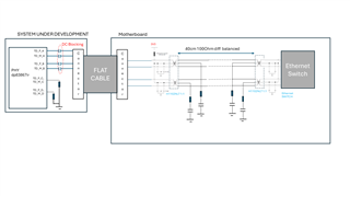
We are developing prototype whose ethernet connection is based on the DP83867IRRGZR.

The solution needs to be plugged to a rather unconventional system that has been designed with Phy (DP83822i) and magnetics split in two boards.

In the original system, the differential pair is generated in the board to be plugged and is sent to the main board via a dedicated flat cable in violation of every recommendation from TI.

The magnetics CT in the mother board is connected to a positive supply as it is requested by DP83822i. This is a problem for the DP83867IRRGZR which works in voltage mode.

A solution we've been talking about is to break the DC-path between the PHY and the transformer with unpolarized capacitors. Do you believe this can work?

Which value would you suggest for the capacitors?

Best Regards, 

GZ

  • Hi GZ,

    We have not seen setups like this in the past, so it's likely this will need to be validated on your end.

    Can you share a block diagram/schematic with the connections so I may further understand and discuss with team?

    Thank you,

    Evan

  • Hello Evan, 

    thank you for your support. Here's a block schematic stressing the interaction between our system and the motherboard we are supposed to plug to.

    The Motherboard cannot be changed, and we need to have the phy compatible with onboard architecture.

    the Phy goes to an ethernet switch through a couple of 1:1 transformers and the first transformer is center tapped to 3V3, which makes it incompatible with the phy we are exploiting.

    Here are our questions:

    # Can we exploit blocking capacitors as shown in the picture below to reach the compatibility?

    # If your answer is positive, can you suggest a suitable value for the blocking capacitors?

    # Can you see any issues with the signal integrity considering this unconventional architecture?

    Is the phy (working in voltage mode) able to manage this setup?

    Thanks in advance for your feedback and support.

    Best Regards, 

    GZ

  • Hi Giulio,

    Thank you for sharing further details on your system. I am reviewing with team, please allow me until Friday to get back to you with feedback.

    Best regards,

    Evan

  • Thank you, Evan, 

    Can you please give us, with the review, some insight about the best way we can (objectively) assess the robustness of the link?

    Another question:

    For the future, supposing we wanted to design a different platform based on the same idea of motherboard with several daughterboards plugged in, each one with an ethernet connection...

    Compared with this solution would it be better:

    #to have both phy and magnetics on the daughterboard,  exporting the analog output through the flat cable?

    #to export the MAC signals, carefully balanced, through the flat cable, having phy and magnetics on the motherboard?

    What option would be better in terms of performances and signal integrity?

    Regards, 

    G


  • Hi Giulio,

    #to have both phy and magnetics on the daughterboard,  exporting the analog output through the flat cable?

    This is the recommended option, as MDI trace length has layout restrictions that may be challenging to meet if the PHY and ethernet connection are on separate boards.

    #to export the MAC signals, carefully balanced, through the flat cable, having phy and magnetics on the motherboard?

    Is the ethernet connection on the motherboard in this case? I'm unclear on the purpose of the daughter board for this setup.

    Looking to give more feedback on your system tomorrow.

    Thank you,

    Evan

  • Hello, 

    Let me recap:

    the motherboard is a multisite that can host a number of daughterboards.

    Each daughterboard (DB) is connected to the MB via a flat cable, so there are as many flat connectors as the number of DB that can be plugged in to the MB.

    The DB is supposed to have the phy but not the magnetics (two of them as you can see in the block schematic), the first of which, located right after the flat connector on the MB, is center tapped to +3V3 because the MB has been designed for a current-mode phy. 

    All the ethernet from the second magnetic are connected to a switch that goes to the global Eth connector.

    In addition to your review of the block schematic, in which DC-Blocking capacitors are placed after the phy to have compatibility phy-magnetics, we need

    #your assessment of the actual connection scheme,

    #info about the actions we can take to assess the quality of the link 

    #your feedback about which option would be better in our case for the placement of Phy and magnetics (present case, both in the DB, both in the MB).

    Thank you again for your valuable support!!!.

    G

  • Hi Giulio,

    It's unclear to me and the team whether this will work, we have not had experience validating this type of setup before.

    # Can we exploit blocking capacitors as shown in the picture below to reach the compatibility?

    It's possible, however there may need to be multiple HW iterations to validate which capacitor value sets the DC offset appropriately.

    # Can you see any issues with the signal integrity considering this unconventional architecture?

    Yes, especially if this is a gigabit application. MDI trace routing requirements are particularly strict, so I'm hesitant to recommend anything outside of what we have explicitly validated.

    #info about the actions we can take to assess the quality of the link 

    The PHY has an internal SQI register that can be used to assess link quality. In addition, it may also help to probe the signal on the PHY-side to confirm the appropriate voltage levels and timing requirements.

    #your feedback about which option would be better in our case for the placement of Phy and magnetics (present case, both in the DB, both in the MB).

    Layout is the main consideration for this. Which option do you envision will reduce the complexity for minimizing trace lengths and length-matching?

    Thank you,

    Evan

  • Hello Evan, 

    Giulio Zoppi said:

    # Can you see any issues with the signal integrity considering this unconventional architecture?
  • Hi Giulio,

    Thanks for clarifying. If you continue with this implementation and face issues, this debug guide will be a useful reference:
    https://www.ti.com/lit/an/snla246b/snla246b.pdf

    Section 3.5 has details on SQI measurements for each of the 4 channels.

    For future solutions, I recommend having the MDI traces minimized with magnetics and RJ-45 on the same board as the PHY. For the signals to the MAC, this can be on the same board, or extended out with a high-speed connector (within trace routing constraints). Please refer to this layout checklist guide for trace routing requirements:

    https://www.ti.com/lit/zip/snlr048

    Best regards,

    Evan

  • Thank you Evan!!!!