This thread has been locked.

If you have a related question, please click the "Ask a related question" button in the top right corner. The newly created question will be automatically linked to this question.

TIC12400-Q1: TIC12400 MSDI configuration as Analog input

Part Number: TIC12400-Q1
Other Parts Discussed in Thread: TIC12400,

Hello team,

I am planning to use TIC12400 in our BCM product , I have confusion configuring it as Analog input , Please look into my below questions and provide the solution.

Is it possible to configure all 24 inputs as ADC .?

What is the maximum Voltage can be applied to the input pin , if it is configured as ADC.?

Is it possible to wake up the MSDI by setting input as Analog threshold?

please consider it as a high priority.

  • Hello,

    Yes, it is possible to use the ADC for all 24 inputs. For reference, see 8.2 "Functional Block Diagram" and section 8.3.8.2 Input Mode Selection, "Each input of the TIC12400-Q1 can be individually programmed to use either a comparator or an ADC by configuring the appropriate bits in the MODE register depending on the knowledge of the external switch connections."

    The maximum voltage that can be applied can be seen in in "6.3 Recommended Operating Conditions", where VINX IN0 to IN23 input voltage has a max input voltage of 35V. However, it should be noted that the ADC full-scale range is 0 V to 6 V.

    The “wake-up” feature is considered normal operation can be configured to assert the interrupt pin when it detects a state change. For example, if an input changes state, then the MCU would see this and read the status registers to see which input had a state change.

    Regards, Amy

  • Hello Amy,

    Thanks for your reply, I have some questions w.r.t ADC threshold.

    below are my requirements.

    Logic low* in digital mode 3.5 V

    Logic high* in digital mode 7.7V

    Max voltage 28V

    Wetting current 10mA

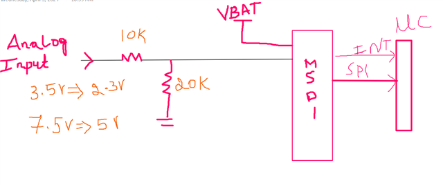
    Considering the above requirements, I will design a Voltage divider before the input pin such that when my Analog Voltage is 3.5V , voltage on the INX pin will be 2.5V and when

    the voltage 7.7V , voltage on the INX will be 5V. whether the MSDI will be able to wake up by setting a threshold when the voltage on INX pin is >=5V and transfer the digital bits to MCU through SPI.

    When the Voltage <=3.5V on INX pin of MSDI by setting a low threshold , is it possible to put the MSDI to pooling mode.

    Unfortunately I was not able to post the image

  • Hi Darshan,

    The inputs to the MSDI device are connected to current sources. Inputs IN0 to IN9 can be programmed to monitor either ground-connected or battery-connected switches (by configuring the CS_SELECT register). Section 8.3.8.1-2 in the datasheet describes the input mode selection. Digital switch inputs are only open or closed, so consider using the comparator option.

    Resistor coded switches can detect multiple positions, and this is where the ADC feature is useful. Using the comparator will reduce polling time and save power. Section 8.3.8.4 provides an overview of the threshold adjustment for a comparator input mode. Section 8.4.2 in the datasheet describes polling mode and links to the conditions of microcontroller wake-up (section 8.3.9.3).

    Regards, Amy

  • For what you are looking to implement, refer to Figure 82. This contains the second use-case for the TIC12400 to monitor analog input from external sensors. The available comparator thresholds are 2V, 2.7V, 3V and 4V, so the voltage divider will need to scale such that a low will be below the chosen comparator threshold. (as described in 9.2.2 Detailed Design Procedure - datasheet pg. 125)

  • Hello Amy,

    Thanks for the quick reply,

    I need to understand more about threshold setting

    Inputs IN12 to IN17 use 2 preset threshold levels (THRES2A and THRES2B).- what is voltage Value that indicates those two registers.

    THRES2A = _ V?
    THRES2B = _ V?

    Similarly whats is the Voltage value that indicates other registers.

    THRES3A, = _ V?
    THRES3B,= _ V?

    THRES3C= _ V?

    If these information  is available in the data sheet , kindly request you to provide the details.

    If possible Please  can you provide me your email ID so that I can send a mail directly.

  • Hi Darshan,

    Sounds like you would like to use the device in ADC mode if you have an analog input. The main thing you need to consider in your design using this configuration is the device leakage current (see pg. 7, the IN_LEAK_0 mA parameter). Place a 15 nF cap near the pin to filter out this leakage current. When an input is configured as ADC input mode, the threshold level for interrupt generation can be configured, up to 1023 different levels, by setting the THRES_CFG1 to THRES_CFG2 registers (Please refer to the datasheet "8.3.8.4 Thresholds Adjustment"). Also refer to the register map details on e THRES_CFG1 to THRES_CFG2 to configure the thresholds for your application.

    If you have additional questions, please accept my E2E friend request and send me a DM message.

    Regards, Amy

  • Hello Amy,

    THRES_CFG1 to THRES_CFG2 are two registers used for Input IN0 to IN11. But for inputs IN12
    to IN17 use 2 preset threshold levels (THRES2A and THRES2B) and similarly other Inputs IN13 to IN23 use present threshold.

    So what will be the value(voltage) of Preset threshold for other inputs from IN12 to IN23.

  • Hi Ashwaththi,

    THRESMAP_CFG0 holds the 8 possible ADC values for the first IN0-IN11 input pins. These ADC values can be compared against a common threshold value (i.e., THRES_COM). This means an interrupt can be triggered if the value in THRESMAP_CFG0 is above or below the THRES_COM.

    For pins IN12 through IN17, you can set up to 8 ADC threshold values in the THRESMAP_CFG1 register. For each input 12 through 17, threshold values can been chosen for 2A and 2B such that the input will either fall below a threshold, between the thresholds, or above the thresholds.

    This idea extends to inputs IN18-IN22, where the input values can fall above / below the threshold levels, and IN23 has the most threshold options.

    Hopefully this helps clarify, I recommend reading section 8.3.8.4 Thresholds Adjustment and following the guidelines on selecting the threshold values (Table 2: Proper Threshold Configuration for ADC Inputs). Additionally, please refer to this application as a supplemental resource: Steps to Configure TIC12400-Q1 Multiple Switch Detection Interface (MSDI)

    Regards, Amy

  • Hello Amy ,

    Thanks for your solution , I do understand the register setting and mapping based on your suggestions.

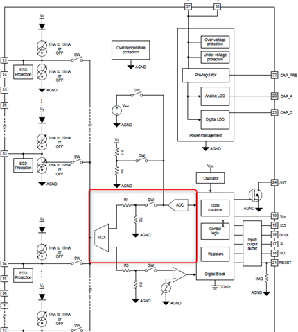
    I have a confusion on ADC Voltage to the input pin.Please refer a below attachment of data sheet block diagram.

    referring to the marked part of diagram, I can see an Voltage divider R1 and R2 integrated to the chip , based on this I have few questions.

    does this Voltage divider internally scale down my input voltage on INX pin to 6V and give it to ADC block or do I need to scale down my voltage to 6V at the input by resistor divider ? if it is not , what is the purpose of these resistors and what is the value of this resistors?

  • Hi Darshan,

    The R1/R2 divider is always a divide-by-two ratio for regular inputs, as listed under the "Rratio" parameter in the datasheet. The device handles the scaling internally and returns a code based on the INx pin voltage where the max code corresponds to 6V. From a user perspective, you don't need to worry about this. The ADC range is defined based upon the external circuitry.

    Regards, Amy

  • Hello Amy,

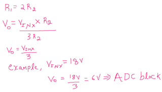
    according to Voltage divider ratio, VINX voltage will be divided by a factor of 3, Please refer the below calculations based on my assumption.

    If my assumptions are wrong, please provide the correct calculations.wihich will speed up our design.  

  • Hi Darshan,

    Thank you for sharing this. Based on lab measurements, this resistive divider is in the range of 120k = R1 = R2, equating to a divide by 2 ratio as shown in the datasheet. Hope this helps clarify.

    Regards, Amy