This thread has been locked.

If you have a related question, please click the "Ask a related question" button in the top right corner. The newly created question will be automatically linked to this question.

DP83826E: Please review the schematic, and some questions.

Part Number: DP83826E
Other Parts Discussed in Thread: AM62A7,

Dear TI experts,

My customer drew their schematic with DP83826E, which is connected to AM62A7.

Could you review this schematic first?

3487.DP83826E.pdf

And here are more questions.

1-1. They want to insert additional connector to connect EVM which can support RGMII (1Gbps) interface.

In this case, Can my customer make through hole on signal line of RMII? (the point which refers red arrow in Q1.)
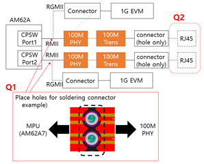
1-2. If yes for question 1, Should my customer disconnect RMII interface if they connect RGMII interface instead?

1-3. Should my customer make a routing with 100ohm differential routing or same length routing (or both?) between AM62A7 and DP83826E?

2. My customer will use the ethernet cable like the picture below.
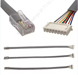
(53261-0871 is the connector for this 1*8 array cable.)

Before production, Can my customer use another RJ45 connector only for the test? this RJ45 connector will be removed before production.

Is it okay to draw schematic like the pdf file above? or Do you have better solution for thest?

Best regards,

Chase

  • Hi Chase,

    Regarding the schematic review, please share this schematic checklist with the customer to fill out:

    https://www.ti.com/lit/zip/snlr050 (BasicMode SchematicChecklist sheet)

    I can help provide help provide further feedback after this is returned.

    Q1: We do not recommend using through holes on RMII signal path. The impedance discontinuity from this is likely to cause issues with the high-speed MAC signals.

    Q2: This is okay, as long as both end-points have the appropriate terminations.

    Thank you,

    Evan

  • Dear Evan,

    Thank you for your support.

    I will get back checklist file asap.

    and here is more question,

    Q1: do not recommend using through holes on RMII signal path. The impedance discontinuity from this is likely to cause issues with the high-speed MAC signals.

    -> Could you recommend designing the schematic to test RGMII interface on the PCB which is already have RMII interface?

    Best regards,

    Chase

  • Hi Chase,

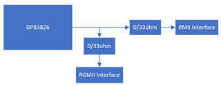
    For testing both RGMII and RMII interface on the same board, 0/33ohm (based on trace impedance) resistors can be put in line and populated to switch between the interfaces:

    Please note the layout restrictions are strict for RGMII/RMII, there may be challenges meeting timing requirements while including layout for both interfaces.

    Here is a layout checklist for reference:

    IndustrialPHY_Layout Review Checklist.xlsx

    Thank you,

    Evan

  • Dear Evan,

    Thank you for your support.

    1. I think that DP83826 is typo in the diagram above, It should be AM62A7 or other processor. And DP83826 is equal as RMII interface. Am I right?

    2. You mean that I can put 0 ohm or 33 ohm in every signal line, based on trace impedance.

    And I should remove the opposite side of all resistors if I test one interface.

    3. And one more question,

    Is there any recommended place to put these resistors?

    (i.e. close to DP83826? or close to each interface?)

    Please check these issues. Thanks

    Best regards,

    Chase

  • Hi Chase,

    1. I think that DP83826 is typo in the diagram above, It should be AM62A7 or other processor. And DP83826 is equal as RMII interface. Am I right?

    Yes, thank you for the correction.

    2. You mean that I can put 0 ohm or 33 ohm in every signal line, based on trace impedance.

    And I should remove the opposite side of all resistors if I test one interface.

    That is correct, only one interface should have resistors populated at a time.

    Is there any recommended place to put these resistors?

    There is no specific restriction for this, however it may be helpful to have them close to the PHY/processor to serve as probe points when validating the signal on input/output.

    Thank you,

    Evan 

  • Dear Evan,

    Thank you for your support, and hope you had a good weekend.

    Here is the checklist file from my customer. Please check it, and please review the schematic.

    DP83826_Schematic_Checklist (S).xlsx

    Best regards,

    Chase

  • Hi Chase,

    Thank you, hope you had a good weekend as well!

    The returned checklist looks good, I have some additional notes on the schematic:

    • Is the LED connection on pin28 intended as a strap? If RMII is being used, add a direct 2.49k PU to enable RMII mode
    • What is the clock rate on XI?
      • If slave mode is intended with 50M XI, strap pin18 with 2.49k PU
      • If master mode is intended with 25M XI, pin18 can be left at default setting

    Best regards,

    Evan