This thread has been locked.

If you have a related question, please click the "Ask a related question" button in the top right corner. The newly created question will be automatically linked to this question.

SN65C3232E: Line driver output has high frequency spikes

Part Number: SN65C3232E

Hello design team

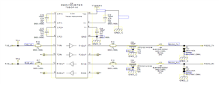
We use SN65C3232EPWR as RS232 line driver in one of our customers product.

sometimes we found ICs which are giving garbage values at its driver output.

further we analyze output using an oscilloscope and found high frequency spikes

present at the output. This problem occurs small fraction of ICs which is about

25% from a lot. please help to solve this problem.

Thanks

Thusith

Electronics Engineer

  • Hi Thusith,

    Can you provide a schematic for us to review? 

    Can you show us the scopeshots of the issue you are seeing?

    Can you also probe the V-/V+ pins of the device and make sure they aren't drooping/collapsing?

    -Bobby 

  • Hi Bobby

    Sorry for late reply!

    Please find schematic diagram below.

    TXD_uC is connected to UART_Tx of STM32 microcontroller. The waveform is measured at RS232_TX.

    Vcomms is at +3.3V

    Garbage value reception and associated wave forms are demonstrated in below video.

    I have done an analysis about failed and passed ICs and here I am sharing the result with you.

    Analysis steps that I followed are listed below:

    1.    First 100 ohm resistor R16 removed from the board.
    2.    Then adjustable power supply E36103A was connected to pin11 of U4 (+) and ground (-).
    3.    Oscilloscope was connected to RS232_TX and ground.
    4.    Board was powered up with 12VDC power supply. (+3.3V at Vcomms)
    5.    While changing  E36103A output, waveform on the oscilloscope was observed.

    In the case of passed IC this video was obtained.

    Input voltage gradually goes down and at 1.219V, output jumps to positive.
    Again input voltage increases gradually but there is no change in output until 1.500V. once 1.5V reaches output jumps back to negative.

    In the case of failed IC, observations present in below video.

    Approximately at 1.062V output shows spiky behavior and as input decreases spikiness becomes critical.
    At about 1.019V spikes disappear and output is  completely transferred to Positive level.
    In this case no transfer threshold can be observed. Instead, transfer happens in a very noisy manner.

    Please advise

    Thanks

    -Thusith

  • Pin 11 is a digital input; you must not try to apply analog voltages to it. The output is defined only for valid logic levels, i.e., for voltages near 0 V and 3.3 V.

    Pin 10 must not be left floating.

    This device already handles the RS-232 bus voltages/currents; remove R18 and R19. (But this is not related to this problem.)

    Please show an oscilloscope trace with both pin 11 and pin 14, with a valid UART input signal.

  • Clemens,

    Thanks for the help!

    Thusith,

    Another expert will get back to you by end of business 04/19/2024.

    Regards,

    Eric Hackett

  • Hi Thusith,

    I agree with Clemen's comments. 

    Pin10 (Tin2) should not be floating. 

    The output waveform in your first video looks like it is swinging to both rails properly without collapsing so I don't necessarily think it's related to the switching caps just yet. 

    I do think we should look at this with two probes on the o-scope. One on the TTL input side (TXD_U) and one of the cable output (RS232_TX). We want to verify the input isn't inputting noise which gets picked up and sent on the output. 

    When the mcu isn't driving the TXD_U net, is there any kind of pull up resistor on the net to ensure its stays at a 5V logic? Or are you sure the MCU is actively holding the TXD_U net high when it's idle?

    Other comments:

    Do you have any decoupling caps on the Vcc pin for our device?

    On a routing perspective, is there any high frequency or high current switching happening under the T1IN/T1OUT traces?

    Thanks,

    -Bobby

  • Hi Bobby and Clemen

    Thanks for your reply!

    the waveforms of signals while communication happens are in below videos.

    1. In case of failed IC.

    at the beginning only RS232_Tx is connected with oscilloscope.

    you can see high frequency spikes appear in the wave form once communication begins. simultaneously monitor at the back

    shows series of garbage values written to terminal window.

    At time 00:30 video shows both signals are connected with oscilloscope. RS232_Tx with trace1 (yellow) and TxD_uC with trace2 (green)

    surprisingly after connecting oscilloscope probe with TxD_uC (pin-11) abnormal behavior disappeared. no spikey waveform on oscilloscope. no garbage on terminal window. at the end still waveform can be observed.

    2. IC having normal behavior

    waveforms obtained from good IC are in Below video

    here anything abnormal is not present.

    "Do you have any decoupling caps on the Vcc pin for our device?"

    Yes, there are several 100nF caps on Vcomms rail. but some of them are shared with another chip.

    "On a routing perspective, is there any high frequency or high current switching happening under the T1IN/T1OUT traces?"

    No, ground plane is directly underneath this chip.

    "When the mcu isn't driving the TXD_U net, is there any kind of pull up resistor on the net to ensure its stays at a 5V logic? "

    No, there is no any pull-up resistor in between MCU and Tranceiver.

    Additional Information:

    we have checked input impedance of pin-11 of good IC and bad IC.

    we have used Fluke 115 multimeter for this purpose.

    Good IC shows around 2.9Mohm resistance from pin-11 to Gnd.

    Bad IC shows around 2.3Mohm resistance from pin-11 to Gnd.

    Hope this fact might be useful.

    Thanks

  • The schematic is incomplete. Please show everything that is connected to the TXD_uC line. Also tell us how the microcontroller's output pin is configured (low, high, or Hi-Z) when the UART output is idle. (I suspect that the line is floating. In that case, a pull-up resistor would help.)

  • Hi Thusith,

    surprisingly after connecting oscilloscope probe with TxD_uC (pin-11) abnormal behavior disappeared. no spikey waveform on oscilloscope. no garbage on terminal window. at the end still waveform can be observed.

    This seems to indicate that this may likely be due to noise or something coupling onto the input pin (TXD_uc) and the mcu isn't holding the output to this net (I suspect it's high-z or a very weak pull down. In most set ups I see, this pin is held HIGH and usually has a weak pull up resistor to hold it high until the MCU is powered and ready to actively drive the pin.

    I think you may want to try putting a 10k or 4.7k pull up resistor on the pin and rerun your testing to see if you still see the issue. Adding a small 100pF cap on the pin can also help filter out any noise that appears on the pin.

    As for why you see one device seeing the issue and not the other, I suspect has to do with silicon variations (doping levels) due to different fab sites and lots.

    -Bobby

  • Hi Bobby

    I will pass these information to the customer and ask his decision about these modifications.

    We noticed that passed and failed components have different part markings as mentioned below.

    Part marking: MU232E-2AK-CQ6J 

                          These components give errors at communication. also driver input impedance show as 2.3Mohm

                          which is relatively low.

    -----------------------------------------------------

    Part marking: MU232E-25K-AZ8R

                         These components work perfectly.  driver input impedance is relatively high. (2.9Mohm)

    I have few more questions:

    • Dose this full part marking refers to different electrical properties of components?  because customer is asking the exact part marking to be used.
    • Does this driver input has some kind of hysteresis band built-in ?
    • Can I arrange shipment of good and bad sets of samples for in house testing ?

    Thanks

    Thusith

  • Hi Thusith,

    Dose this full part marking refers to different electrical properties of components?  because customer is asking the exact part marking to be used.

    There was a die revision for this device issued in 2021 of June. Based on the part markings I was able to verify both parts appear in our internal look up system and both devices are the 'new' die. This means both devices should be the exact same. (Maybe some minor silicon variation between lots)

    Does this driver input has some kind of hysteresis band built-in ?

    Generally our design teams don't build an external hysteresis circuit into CMOS inputs unless they need a very high level of sensitivity built in. They usually use some kind of internal overlap between the NMOS and the PMOS which usually gives a very small amount of hysteresis in the order of double digit mV. 

    Can I arrange shipment of good and bad sets of samples for in house testing ?

    Do you have a TI representative for your company? Normally you would communicate with them on a potential concern for retesting. Based on my understanding, the input you have is likely floating so based on a system level they may not accept the request. They would only accept requests like this if they believe a quality issue has occurred. 

    -Bobby

  • Bobby,

    Thanks for your support given so far to solve this issue.

    i will contact the customer with your information and try to solve this issue.

    If there is a doubt i will get back to you later through this forum.

    Thanks, bye!

    Thusith