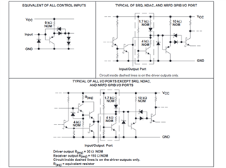
Part Number: SN75161B

Folks,
The above is a snipped form the SN75161 datasheet. (BTW I know this is going obsolete.)
The picture shows the tpyical ports for both kinds of lines. I don't understand it; these are bidirectional ports so they must have an input and an output, but these figures simply say "input/output port". So what is that, the part that's at the outside world? The part that connects to the micro (the local bus)? Either way up, where is the OTHER end of the connection? So if it's configured as an input, where is the ouput and vice-verse?
Also, the input and output labels look the wrong way round. If you look at the SRQ/NDAC & NRFD port, these need to be open collector, but the open collector is on the left hand side of the diagram, which is labelled input. However, to further confuse things, it says the circuit inside the dashed lines is the output. So which is it? Should the "Input/Output Port" label say "Output/Input Port"? And, as I say, is that in respect to the GPIB bus or to the local logic?
Also, it talks about "driver output" and "receiver output" what is driver and what is receiver? Is driver sending the logic signals to outside world (ie the GPIB bus)? Or is this dependent on the direction set by the DC pin? Is that resistor changed dependent on the state of that pin?
I'm clearly missing something fundamental here and completely failing to follow this datasheet!
Thanks.

