This thread has been locked.

If you have a related question, please click the "Ask a related question" button in the top right corner. The newly created question will be automatically linked to this question.

THVD1406: Low impedence problem between 5V supply and the 3.3V used as pull-up for the UART side level of the device

Part Number: THVD1406

Hi TI Team,

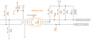
I'm selecting THVD1406 as a 485 autodirectional transceiver for a new product and I have found the following problem on the PCB prototype:

there's a low impedence path between the +5V rail and the +3.3V caused by the turn on of D1 protective diode. Attached you can see the schematic.

I think that the origin of the problem is that in default R pin goes to 5V and this turns on D1.

Anyway I need 3.3V on the UART side of the transceiver because the MCU  UART pins don't accept higher voltage levels.

Should one solution be to supply THV14006 with 3.3.V? In this case, which are A-B differential voltage output levels? Should they swing between -3.3V(as negative voltage) and 6.6V (as positive voltage)?

My concern is not to lower so much the A-B differential voltage output levels using a 3.3V supply compared to 5V supply.


Or maybe  another solution is to keep 5V supply is adding a series resistor between R and anode of D1 to make a voltage divider?

Thank you for the support

Alessandro

  • You would need a level shifter to prevent the 5 V signal from reaching the MCU.

    For the differential output voltage, see the |VOD| specification. It's smaller at 3.3 V, but should still be large enough.

  • Hi Alessandro,

    I think that the origin of the problem is that in default R pin goes to 5V and this turns on D1.

    Correct. The R pin of the THVD1406 is a CMOS output that drives high to ~Vcc. So when the logic is HIGH it will drive from the R pin into the diode into the 3.3V rail that you currently have set up. 

    Should one solution be to supply THV14006 with 3.3.V? In this case, which are A-B differential voltage output levels? Should they swing between -3.3V(as negative voltage) and 6.6V (as positive voltage)?

    My concern is not to lower so much the A-B differential voltage output levels using a 3.3V supply compared to 5V supply.

    This device does support 3.3V on Vcc. The output on the A-B pins will be a bit weaker but for the most part still work. The device itself does not generate voltage swings in the way that you are thinking. It basically drives current through a termination resistor to generate a voltage. RS485 standard dictates that the output drive should be larger than 1.5V across a 54 ohm load. The negative polarity of this differential voltage comes from driving the current into the resistor in the opposite direction. RS485 is essentially an H-bridge driver where the 'load' is the termination resistance. Using 3.3V for Vcc should work in most instances. 

    Or maybe  another solution is to keep 5V supply is adding a series resistor between R and anode of D1 to make a voltage divider?

    Using a level translator would probably be better since it lowers power. Using a voltage divider can work against you if the capacitance of the R load is too large or need to switch quickly (voltage dividers forms and RC circuit). Would depend on the R values you choose.

    I personally think changing the Vcc of THVD1406 to 3.3V would be the easiest solution here. 

    -Bobby

  • Thank you for your answers.

    When you say "Using a level translator would probably be better since it lowers power" you mean to add a series resistor between R pin and R5 of about 50Kohm for lowering the voltage which is connected to MCU?

    Another question: is my configuration with RE/ and SHDN/ pins both pulled high by 10KOhm correct for using the device in auto-direction mode?

    Thank you for your support

    Alessandro

  • When you say "Using a level translator would probably be better since it lowers power" you mean to add a series resistor between R pin and R5 of about 50Kohm for lowering the voltage which is connected to MCU?

    If you go the resistor divider way, you would put a resistor infront of the Rpin and then another resistor connected to the previous resistor and GND. If R5 is populated then you would need to account for that during the HIGH state of the divider. 

    Note: the resistors you choose will affect the RC. Using large ones may cause signal integrity issues at higher datarates.

    Another question: is my configuration with RE/ and SHDN/ pins both pulled high by 10KOhm correct for using the device in auto-direction mode?

    Yes #SHDN should be enabled for auto-direction to work when transmitting data. The #RE pin state doesn't affect auto-direction but you should be aware that the device will still feed data from the cable into Rx even when #RE is held high after the auto direction timer has expired.

    "When RE is logic high or left open and D input switches from logic low to logic high, the receiver output is high-impedance for the duration of tdevice-auto-dir. After the duration of tdevice-auto-dir, the receiver turns ON and outputs a logic high or low depending upon the differntial bus input voltage"

    -Bobby

  • Hi Bobby,

    yes I see.. Assuming #SHDN  pulled high, which is the difference between pulling RE/ high or low?

    Reading the datasheet, It seems that also keeping  #RE low the R pin follows the VID (A-B differential pins voltage) and the only difference is not waiting tdevice-auto-dir when D changes from low to high before enabling R pin.

    Am I correct? 

    Thank you for your help

    Alessandro

  • Reading the datasheet, It seems that also keeping  #RE low the R pin follows the VID (A-B differential pins voltage) and the only difference is not waiting tdevice-auto-dir when D changes from low to high before enabling R pin.

    Am I correct? 

    Correct. 

    I should also ask, is there a reason why you didn't set the Vcc for this device to 3.3V? 

    I feel like that would of cleaned up a lot of the circuitry you have on the right hand side of your schematic. The device itself can support Vcc=3.3V and the cable side circuitry wouldn't need to be modified.

    -Bobby

  • Hi Bobby,

    I was concerned about setting to 3.3V the supply because I thought It would lower the A-B differential output level too much but It was a mistake. (Also your detailed description was helpful for understanding this topic).

    Now I'll use the 3.3V for supplying the device.

    As for cleaning the right hand side of the circuitry with 3.3V supply, I'm not sure if the D1 diode is useful to protect R pin (and hence thUART0_RX_SLAVE pin of MCU)..what do you think about this?

    The other resistors (R4,R5,R6,R8) should be kept on the schematic for handling the idle trasmission and receiver states, correct?

    Thank you for your support,

    Alessandro