Part Number: TMDS181
Dear team,
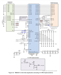
We have use TMDS181 in our application, but face to some issue.
Could you share your feedback about below questions?
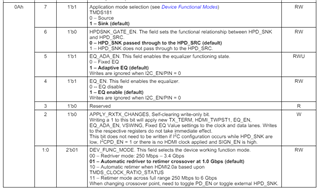
1. Can we manual control TMDS181 operate in bypass mode (as redriver)? no matter the data rate.
If yes, how to set the mode?
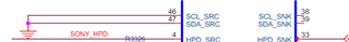
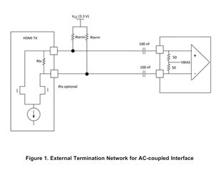
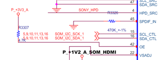
2. Please help to review the schematic and share your feedback if any risk.
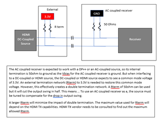
input spec for your reference

Thanks,
Ben