This thread has been locked.

If you have a related question, please click the "Ask a related question" button in the top right corner. The newly created question will be automatically linked to this question.

TCAN4550-Q1: TCAN4550-Q1 40MHz Oscillator requirement

Part Number: TCAN4550-Q1

I have a board with a TCAN4550-Q1 component, connected to a 40 MHz Crystal

During testing, I saw in DS that the OSC1 Terminal requires the input level as follows (marked in yellow):


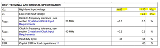
What does this requirement mean?

What are the units VIO?


For example, I have the following signal (attached Pic) I have measured in the OSC1 terminal:

VIH= 1.204V

VIL= 0.564V

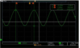
Does this signal meet the requirement from the table?

  • Hello Matan,

    The TCAN4550-Q1 can work with either a crystal or a single-ended clock input.  The VIH and VIL specifications are for the Single-ended clock option which you are not using.  VIO is the voltage level connected to the VIO pin which can be either 3.3V or 5V typical and this voltage sets the digital signal voltage levels.  Therefore, the single-ended clock input High and Low specifications are relative to the VIO voltage.

    For example if VIO = 3.3V then:

    VIH(min) = 0.85 x 3.3V = 2.805V

    VIH(max) = 1.1 x 3.3V = 3.63V

    VIL(max) = 0.3 x 3.3V = 0.99V

    However, because the TCAN4550-Q1 supports both a crystal and a single-ended clock, there are some extra considerations and optimization needed to ensure it does not switch between these clock modes during normal operation.  Please read the TCAN455x Clock Optimization and Design Guidelines application note for more information (Link).

    The OSC1 signal of your crystal looks fine, but more important is the OSC2 signal levels.  The TCAN4550-Q1 uses a comparator on the OSC2 pin to detect a "Grounded" pin condition or a voltage less than 150mV (max) as an indicator that the device should use a single-ended clock and disable the crystal current amplifier.  If the voltage on the OSC2 pin waveform drops below this threshold, then the device may disable the crystal and switch to single-ended clock mode which may cause some CAN and SPI communication errors to occur.

    Regards,

    Jonathan