


Part Number: TSD05
Hello E2E Engineers,
I am seeking your expertise to review my PCB layout designed for robust ESD protection in an industrial environment. Below are the details of my configuration:
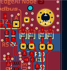
- TVS Diodes: TSD05, placed close (2mm) from the input connectors.
- Signal Characteristics: 4 x 5V digital inputs, ~10kHz maximum frequency, with trace lengths under 5cm.
- PCB Details: Two-layer board with a 1.5mm FR4 dielectric.
- The bottom layer is a solid ground connected directly to the power supply return.
- The top layer has a dedicated ESD ground plane near the connectors, connected only to TVS diode ground pins.
- This plane is linked to the bottom ground layer via approximately 40 vias (0.35mm drill hole, 0.6mm annular ring) on 60micron copper layers. - Grounding Strategy: The isolated top ESD ground plane is intended to act as a buffer during ESD/EOS events, distributing the charge across its area to minimize impact on other components. All ICs on the PCB are decoupled.
- Trace Details: Input to TVS diode traces have teardrops, with a minimum width of 0.6mm; traces to the MCU are 0.2mm wide, with a standard 0.25mm separation across the board.
- Filter Components: The resistor in the RC low-pass filter is placed in series on the trace close to the connector before passing the incoming signal to the MCU GPIO pin.
I have not yet conducted any tests, so I am particularly interested in understanding potential concerns with this layout, especially related to ESD current distribution towards the TVS diodes and the low-pass filter components.
Attached is the layout of the top layer for your review. I appreciate any guidance or suggestions you might have on whether this layout is advisable and any potential improvements to enhance ESD protection.
Thank you for your assistance!
My particular doubt is the ESD current distribution pattern & relative flow towards TVS diode & the RC LP-Filter components - any guidance here would be highly appreciated.
