HI,Team.
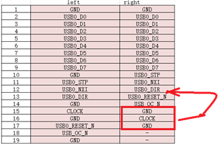
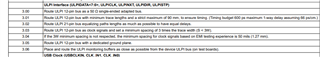
As shown on the left side of the figure below, it is the signal arrangement of the USB ULPI interface on a connector. The pin spacing of the connector is 0.5mm. I want to eliminate a few GND pins because the connector has insufficient pins. Pin 18 is a USB power supply overcurrent detection signal, which is an open-drain signal connected to the GPIO. Pin 17 is the reset signal of USB_PHY. Can the signal arrangement be operated according to the arrangement on the right?Thank you so much.
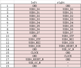
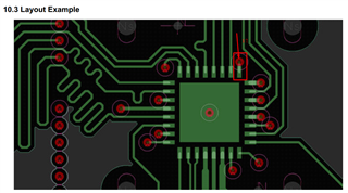
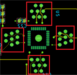
As shown below is the LAYOUT diagram of TUSB1210. The first pin of the IC is the pin in the red box in the picture? The definition of 8, 15, 16, 24, and 25 of this chip is NC. Why are they all wired in the picture? Thank you so much.