This thread has been locked.

If you have a related question, please click the "Ask a related question" button in the top right corner. The newly created question will be automatically linked to this question.

TL16C750E:Compatibility with TL16C750

Part Number: TL16C750E
Other Parts Discussed in Thread: TL16C750

こんにちは。

製品改訂に伴い、製品のUARTをTL16C750からTL16C750Eへの変更を検討しています。

添付図のようにUARTと回路を変更したところ、起動時からSRAMへの書き込みができず、端末が暴走状態になってしまいました。 しかし、TL16C750回路はそうではありませんでした。

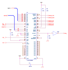
基板からUARTを取り外したところ、正常に動作したので、UART周辺の回路に問題があると思いました。

デバイス起動時にUARTチップセットがディスエーブルされると、データバス端子はハイインピーダンスになりますが、実際にはデータバスは出力状態になっていました。

その後、チップセットを有効にしてデバイスをリセットすると、データバスがハイインピーダンスになりました。

データシートを確認しましたが、チップセットを有効にしてリセットするという記載はありませんでした。

以下の点について教えてください。

・TL16C750とTL16C750Eの相性(端末機能の違いなど)

・起動時やリセット時の挙動についてですが、この挙動は正しいですか?

ありがとうございます。

  • Hello,

    I'm not able to understand the additional information you provided in your post but I do see the title to the post is in english.

    The E version of the TL16C750 has a lot of additional registers. We've seen in the past that when customers try to move from an older device to a newer one, sometimes the new register map additions/rules can cause conflicts with the previous software. 

    We always recommend customers test the new devices to see if their software is compatible, in some cases there are also timing differences that can make the older existing firmware incompatible with the newer device. 

    If you run into issues, we can try to help debug issues you are seeing if you're able to get scope shots and provide some kind of pseudo-code or modify you're existing software. 

  • Sorry. The text had been converted to Japanese.
    Resend.

    Due to product revisions, we are considering changing the product's UART from TL16C750 to TL16C750E.
    When I changed the UART and circuit as shown in the attached diagram, I was unable to write to SRAM from the time of startup, and the terminal went into a runaway state.

    When I removed the UART from the board, it worked fine, so I thought there was a problem with the circuitry around the UART.
    When the UART chipset is disabled, the data bus terminals become high impedance, but the data bus is actually in an output state.
    Then enabled the chipset and reset the device and the data bus became high impedance.
    I checked the datasheet and there was no mention of enabling and resetting the chipset.

    Please tell me about the following points.
    ・Compatibility between TL16C750 and TL16C750E(Differences in pin functions)
    ・Regarding the behavior at startup and reset, is this behavior correct?

  • I checked the datasheet and there was no mention of enabling and resetting the chipset.

    The device should already see a reset when Vcc is ramped up. It is generally a good idea to toggle reset after powering up a heavily digital device. To ensure default values incase a bad PoR does occur.

    ・Regarding the behavior at startup and reset, is this behavior correct?

    I personally haven't seen this kind of issue occur. I would recommend double checking the IOR pin and the Mode pin of the device to make sure IOR isn't LOW and Mode is HIGH. If you are using Mode as LOW, you would want IOW low or CS HIGH. This would be the 2 ways you would have the parallel output pins outputting something. 

    I do know if the device isn't powered and you have any of the input pins like D0-D7 at a logic high level, it can leak/back-bias into the device. 

    ・Compatibility between TL16C750 and TL16C750E(Differences in pin functions)

    I Mentioned this in the earlier post but we don't really guarantee backwards compatibility with the two devices. In the past, what we've seen is sometimes the new registers in the newer device could cause software issues using the older device's firmware.

    -Bobby

  • Hi, BOBBY.

    I personally haven't seen this kind of issue occur. I would recommend double checking the IOR pin and the Mode pin of the device to make sure IOR isn't LOW and Mode is HIGH. If you are using Mode as LOW, you would want IOW low or CS HIGH. This would be the 2 ways you would have the parallel output pins outputting something. 
    I checked and IOR and MODE are HIGH.
    MODE pin is pulled to VCC (3.3V).
    I do know if the device isn't powered and you have any of the input pins like D0-D7 at a logic high level, it can leak/back-bias into the device.
    Before power supply, D0-D7 are all pulled to GND and the logic is LOW.
    It becomes undefined immediately after power-on, and becomes HIGH after initialization processing.
    Continuing to output the data bus causes contention with SRAM, and as a result, writing to SRAM is no longer possible.
    We are currently confirming the changes to the register.
  • We are currently confirming the changes to the register.

    Can you do a register read before the reset and then repeat and read the registers after the reset toggle to verify if you see any changes? 

    Can you also provide the waveform for the Vcc rail when you power up the 750E? I'd like to make sure you're powering up from GND to Vcc within a reasonable time.

    -Bobby

  • Hello, BOBBY.

    Can you also provide the waveform for the Vcc rail when you power up the 750E? I'd like to make sure you're powering up from GND to Vcc within a reasonable time.

    Provides Vcc and D0 waveforms. Yellow is Vcc (3.3V), blue is D0.

    The first image shows the waveform from power-on to reset processing.
    The second image shows the waveform when the power is turned on.

    I will also provide waveforms when CS is shorted to GND at power-up or reset, as I mentioned in my first post.

  • Hi,

    Bobby is out of office at the moment but will return to attend to this inquiry next week. 

    Best,

    Parker Dodson

  • In the image sent last time, D0 fluctuates 200ms after the power is turned on. This wait time is caused by the reset IC, and we have confirmed that it behaves as specified.
    Also, the 750E data sheet recommended a 1µF bypass capacitor, so I changed it to this, but there was no noticeable change in behavior.

  • Hi,

    The power up (Vcc) waveform looks okay to me, from what I can see it seems like it goes from GND to Vcc in about 10ms assuming the divisions are correct.

    The first image shows the waveform from power-on to reset processing.
    The second image shows the waveform when the power is turned on.

    Are you saying the reset occurs before D0 begins toggling or do you mean after it begins toggling?

    From the scopeshot, it does look like the D0 pin may be in contention with another whatever else is tied to the net and driving it low. (pin looks like it's stuck around 2V). 

    For my understanding, 

    When you power up the device for the first time, you see data pins are outputs even when CS is disabled and IOR is held HIGH. If you toggle reset, the data pins become high impedance like you expect them. 

    Is this statement correct?

    -Bobby

  • Are you saying the reset occurs before D0 begins toggling or do you mean after it begins toggling?

    The reset IC maintains operation for 200 ms after power-on, or while the reset button is pressed manually.When not in use, D0-D7 are pulled up to Vcc, which is probably why they are fixed at around 2V.

    For my understanding, 

    When you power up the device for the first time, you see data pins are outputs even when CS is disabled and IOR is held HIGH. If you toggle reset, the data pins become high impedance like you expect them. 

    Is this statement correct?

    Probably so. In the reset state, D0-D7 becomes high impedance and does not return to high impedance after the CPU initialization operation (the part where D0 fluctuates) is completed.

  • I think I may have an EVM for this device laying around. I can try to power up the device and see if the D0 pin is an output before the reset pin is toggled. 

    Just to be sure though, you are seeing the D0 pin acting as an output before reset is toggled or during reset where you hold the device in reset for 200ms.

    -Bobby

  • Just to be sure though, you are seeing the D0 pin acting as an output before reset is toggled or during reset where you hold the device in reset for 200ms.

    During the reset state, the UART CS, IOW, and IOR pins are each pulled up to Vcc. When actually measured, 3.3V (Vcc) was observed for each, so D0-D7 are considered to be in neither an input nor an output state.

  • Thanks for clarifying, I will try to test this in the lab by the end of the week. I'll let you know if I see something similar.

    -Bobby

  • I've tried to repeat what you saw on the D0 pin by holding the reset pin high but I didn't see the D0 pin behave any differently. I saw the D0 pin float to GND before and after reset was toggled.

    I will try again next week and modify my board a bit more and see if that changes anything. 

    -Bobby

  • Hello, BOBBY.

    Regarding the confirmation using EVM, what has happened since then?

    I'd appreciate if you could reply.

  • Sorry I forgot to update you. I tried again but saw the same thing, the D0-D7 pins didn't seem to act any differently when the reset pin was toggled. I'm not sure if this is a set up problem on my side or yours. 

    I could try to order a breakout board and try to repeat the test on that instead if you think this would be helpful. Let me know, I will need to work with my admin to try to order the breakout board.

    -Bobby