This thread has been locked.

If you have a related question, please click the "Ask a related question" button in the top right corner. The newly created question will be automatically linked to this question.

HD3SS3412: HD3SS3412 Power Dissipation Changes

Part Number: HD3SS3412

Hi TI Team,

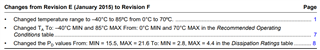
I would like to ask what is the changes on the part why the power dissipation become  MIN = 2.8mW, MAX = 4.4mW? Original rating is MIN = 15.5mW, MAX = 21.6mW.

We used this IC in our board and we created a checker to check the current of the device. Initially, we set the limits to 2mA and 6mA. We fabricated new board, unfortunately, failed on lower limits since the measure current is only 1mA. We replaced the IC several times and still reading is 1mA. Swap the passing and failing IC and failure transferred. Upon checking the datasheet, power dissipation is changed that's why current become 1mA only. I hope you will notice my inquiry.

Thanks,

Cian

  • Hi Cian,

    I believe this was changed due to either a change in the device design or a change in the test setup where this parameter was measured. I can follow up on this with our systems engineer if you'd like.

    Are you able to lower the limit on your current measurement device?

    Best,

    Shane

  • Hi Shane,

    You can take your time. I would love to if we can share the changes on device. 

    I just change the lower limit to 0.848mA = 2.8mW/3.3V based on the new specs on the datasheet.

    Thanks,

    Cian

  • Hi Cian,

    I followed up with systems on this. Back in 2015 we changed the IC inside this device, which allowed a wider temperature range and lower power dissipation. You can see the changes in the datasheet here:

    Let me know if you have any other questions.

    Best,

    Shane

  • Thank you for you reply Shane. We have a follow up question. When you say "IC inside" do you mean that HD3SS3412 is a hybrid device or the die only that changed?

    Other question would be this. We would like to know the trigger behind the change of revision of the IC from rev E to F?

    Is there a design flow that needs to be updated or is this a costumer triggered the changes from rev E to F? Or something else??

    This we would like to know. Thanks.

  • Hi Luciano,

    When you say "IC inside" do you mean that HD3SS3412 is a hybrid device or the die only that changed?

    Only the internal die was changed.

    We would like to know the trigger behind the change of revision of the IC from rev E to F?

    Can I ask why you need this information? I am not aware of the reason for the change myself.

    Is there a design flow that needs to be updated

    The device package was not changed from Rev E to Rev F so there should be no design changes needed between these versions.

    Best,

    Shane

  • Hi Shane,

    We are affaid in the changes of the device die since power reduces almost 500%.
    If the old part is not available anymore, how can we assure that the new die will not damaged in the long run.
    Thats why we are curious on what is the reason why the power reduces by 500%?
    Does the performance of the device affected using the new die? Or only the control pins circuit is changed?

    Thanks,
    Cian

  • Hi Luciano,

    Does the performance of the device affected using the new die?

    The performance of this device is characterized by the values in the datasheet. The only change in device performance from Rev E to Rev F was the power dissipation reduction and temperature range increase. Other than that, the device performance is not affected by the new die.

    If the old part is not available anymore, how can we assure that the new die will not damaged in the long run.

    If you're concerned about long term failure rates, we have a FIT estimator tool you can use to see the tested failure rate of this device.

    Best,

    Shane

  • Hi Shane,

    Thanks you very much for your time.

    Thanks,

    Cian