This thread has been locked.

If you have a related question, please click the "Ask a related question" button in the top right corner. The newly created question will be automatically linked to this question.

PCA9306-Q1: if there is some potential risk when VREF2 directly connect to VDD_3V3?

Part Number: PCA9306-Q1
Other Parts Discussed in Thread: PCA9306

Hi, TI Colleagues

Our one product use the PCA9306 and VREF2 directly connect to VDD_3V3,detail as bleow shows. Currently it pass the DV and PV test. We're wondering if there is some potential risk for this and what's the risk?

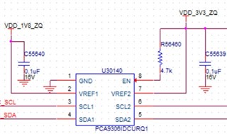
If the FET in chip was damaged because of the large current, what's the failure mode, VREF1 disconnect with VREF2? or VREF1 and VREF2 short together?

  • Hey Gavin,

    There exists an internal passFET between VREF1 and VREF2 that is configured as a diode and becomes forward biased when VREF2 is supplied power. The external 200kohm is needed to reduce current flow through the internal FET of the PCA9306 to ensure that the internal FET does not become damaged, while also reducing the leakage current sinking into VREF1 from VREF2. 

    The leakage current seen on VREF1 side can be denoted as: Ileakage= VREF2-(VREF1+VTH)/ RBIAS with VTH = 0.6V (approx.)

    Regards,

    Jack 

  • Hi, Jack
    Thanks for the information, the test pass with current configuratioin. Our concern is if there is a risk for current design? Will the internal passFET be damaged? And in case of internal passFET damaged, will the VREF1 and VREF2 connect together or disconnect?

  • The channel current must be limited to less than 128 mA. If your 3.3 V supply is strong enough, this can damage the device.

    There is no guarantee what the consequences of damage might be.

    Please note that with EN at 3.3 V, the SCL1/SDA1 output voltages will not be clamped to 1.8 V; all the 1.8 V I²C devices might get damaged.