Other Parts Discussed in Thread: TCAN4550, TCAN4550-Q1
Tool/software:
I have connected the STM32 and TCAN4550EVM and want to enable CAN FD communication. However, there are no signals being transmitted on the CAN H/L lines. How can this be resolved?
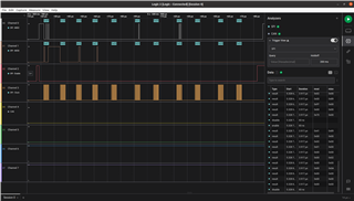
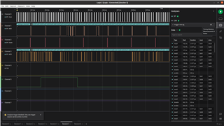
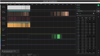
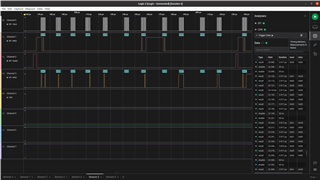
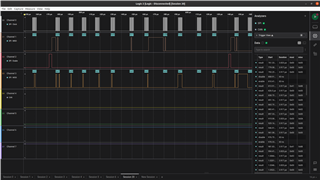
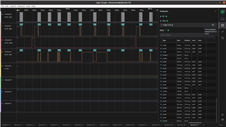
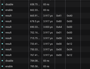
The logic analyzer detected multiple instances of 0x81 and 0x89 on MISO. How can this issue be resolved?
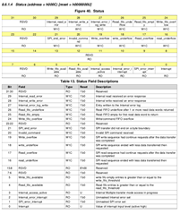
Where can I find information about the error messages returned on MISO?
For HW connection
TCAN4550EVM
- TCAN4550EVM is powered by a DC source through J8(->VSUP) on TCAN4550EVM.
- VIO SELECT(S1) is chosen to be in 5V output.
- CAN H ->CAN H
- CAN L ->CAN L
- light on :
- nINT
- nWKRQ
- D2
- D3
- D4
- D5
- D6
NUCLEO-WB55 LaunchBoard
- spi1_sck -> SPI CLK
- spi1_miso -> SDO
- spi1_mosi -> SDI
- spi1_nss -> SPI CS
- exti1 ->nINT
For SW configuration
- SPI configuration
- The MSP430 uses an 8 MHz clock source, targeting a 2 MHz SPI clock. The STM32 uses a prescaler to set the SPI clock. SPI_BAUDRATEPRESCALER_32 divides the system clock (64 MHz) to 2 MHz.
-
Clock Polarity and Phase: The MSP430 is set to EUSCI_B_SPI_CLOCKPOLARITY_INACTIVITY_LOW and EUSCI_B_SPI_PHASE_DATA_CAPTURED_ONFIRST_CHANGED_ON_NEXT. The corresponding settings for STM32 are SPI_POLARITY_LOW and SPI_PHASE_1EDGE. These settings indicate that the clock is low-level idle, and data is captured on the first edge (rising edge).
-
Data Bit Order:The MSP430 is set to EUSCI_B_SPI_MSB_FIRST. The STM32 is set to SPI_FIRSTBIT_MSB. Both are MSB first
-
Data Size: The MSP430 defaults to an 8-bit data size. The STM32 is set to SPI_DATASIZE_8BIT.
static void MX_SPI1_Init(void)
{
/* SPI1 parameter configuration*/
hspi1.Instance = SPI1;
hspi1.Init.Mode = SPI_MODE_MASTER;
hspi1.Init.Direction = SPI_DIRECTION_2LINES;
hspi1.Init.DataSize = SPI_DATASIZE_8BIT;
hspi1.Init.CLKPolarity = SPI_POLARITY_LOW;
hspi1.Init.CLKPhase = SPI_PHASE_1EDGE;
hspi1.Init.NSS = SPI_NSS_SOFT;
hspi1.Init.BaudRatePrescaler = SPI_BAUDRATEPRESCALER_32;
hspi1.Init.FirstBit = SPI_FIRSTBIT_MSB;
hspi1.Init.TIMode = SPI_TIMODE_DISABLE;
hspi1.Init.CRCCalculation = SPI_CRCCALCULATION_DISABLE;
hspi1.Init.CRCPolynomial = 7;
hspi1.Init.CRCLength = SPI_CRC_LENGTH_DATASIZE;
hspi1.Init.NSSPMode = SPI_NSS_PULSE_DISABLE;
}
- I modified the TCAN455x Driver Library Demo to make it compatible with STM.
void
AHB_WRITE_BURST_START(uint16_t address, uint8_t words)
{
//STM32
// Set the CS pin low to start the transaction
HAL_GPIO_WritePin(SPI1_NSS_GPIO_Port, SPI1_NSS_Pin, GPIO_PIN_RESET);
// Transmit the AHB write opcode
uint8_t WRITE_OPCODE = AHB_WRITE_OPCODE;
if (HAL_SPI_Transmit(&hspi1, &WRITE_OPCODE, 1, 3) != HAL_OK)
{
/* Transfer error in transmission process */
Error_Handler();
}
while (__HAL_SPI_GET_FLAG(&hspi1, SPI_FLAG_BSY) == SET) {}
// Send the 16-bit address
uint8_t address_high = (address >> 8) & 0xFF; // High byte
uint8_t address_low = address & 0xFF; // Low byte
if (HAL_SPI_Transmit(&hspi1, &address_high, 1, 3) != HAL_OK)
{
/* Transfer error in transmission process */
Error_Handler();
}
while (__HAL_SPI_GET_FLAG(&hspi1, SPI_FLAG_BSY) == SET) {}
if (HAL_SPI_Transmit(&hspi1, &address_low, 1,3) != HAL_OK)
{
/* Transfer error in transmission process */
Error_Handler();
}
while (__HAL_SPI_GET_FLAG(&hspi1, SPI_FLAG_BSY) == SET) {}
// Transmit the number of words to read
if (HAL_SPI_Transmit(&hspi1, &words, 1, 3) != HAL_OK)
{
/* Transfer error in transmission process */
Error_Handler();
}
while (__HAL_SPI_GET_FLAG(&hspi1, SPI_FLAG_BSY) == SET) {}
}
while (__HAL_SPI_GET_FLAG(&hspi1, SPI_FLAG_BSY) == SET) {}
}
void
AHB_WRITE_BURST_WRITE(uint32_t data)
{
// Transmit the data bytes in little-endian order
uint8_t dataBytes[4];
dataBytes[0] = data & 0xFF; // Low byte
dataBytes[1] = (data >> 8) & 0xFF; // Byte 1
dataBytes[2] = (data >> 16) & 0xFF; // Byte 2
dataBytes[3] = (data >> 24) & 0xFF; // High byte
// Transmit each byte of data
if (HAL_SPI_Transmit(&hspi1, &dataBytes[3], sizeof(dataBytes[3]), 3) != HAL_OK)
{
/* Transfer error in transmission process */
Error_Handler();
}
while (__HAL_SPI_GET_FLAG(&hspi1, SPI_FLAG_BSY) == SET) {}
if (HAL_SPI_Transmit(&hspi1, &dataBytes[2], sizeof(dataBytes[2]), 3) != HAL_OK)
{
/* Transfer error in transmission process */
Error_Handler();
}
while (__HAL_SPI_GET_FLAG(&hspi1, SPI_FLAG_BSY) == SET) {}
if (HAL_SPI_Transmit(&hspi1, &dataBytes[1], sizeof(dataBytes[1]), 3) != HAL_OK)
{
/* Transfer error in transmission process */
Error_Handler();
}
while (__HAL_SPI_GET_FLAG(&hspi1, SPI_FLAG_BSY) == SET) {}
if (HAL_SPI_Transmit(&hspi1, &dataBytes[0], sizeof(dataBytes[0]), 3) != HAL_OK)
{
/* Transfer error in transmission process */
Error_Handler();
}
while (__HAL_SPI_GET_FLAG(&hspi1, SPI_FLAG_BSY) == SET) {}
}
void
AHB_WRITE_BURST_END(void)
{
// WAIT_FOR_IDLE;
// Wait for SPI transmit buffer to be empty
while (__HAL_SPI_GET_FLAG(&hspi1, SPI_FLAG_BSY) == SET) {}
// GPIO_setOutputHighOnPin(SPI_CS_GPIO_PORT, SPI_CS_GPIO_PIN);
// Set CS pin high to end the transaction
HAL_GPIO_WritePin(SPI1_NSS_GPIO_Port, SPI1_NSS_Pin, GPIO_PIN_SET);
}
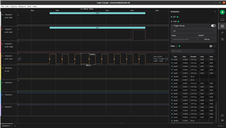
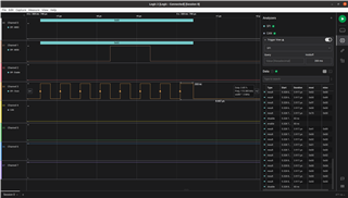
I repeated TCAN4x5x_Device_ClearSPIERR() twice because there was an issue with reading one set of data from the logic analyzer.
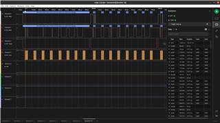
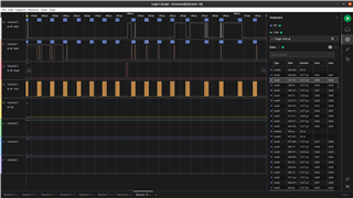
The logic analyzer detected multiple instances of 0x81 and 0x89 on MISO. How can this issue be resolved?
Where can I find information about the error messages returned on MISO?
Where can I find information about light on TCAN4550EVM?