This thread has been locked.

If you have a related question, please click the "Ask a related question" button in the top right corner. The newly created question will be automatically linked to this question.

DS91M125: Can one of the driver output be left open with enable pin active?

Part Number: DS91M125

Tool/software:

Hello,

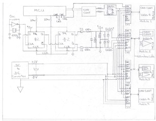
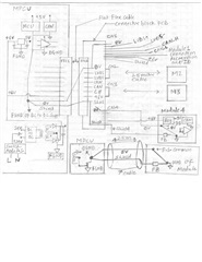
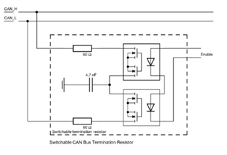
We have a system where LVDS Driver output signal has Vcm = 2.1V with Vid = 1.1V (each LVDS line swings from 2.1V to 2.65V with respect to ground when connected to a single 120 ohm input terminated LVDS receiver through 2.5 meter cable) at 1 MHz that is used as reference clock. It means the Vcm exceeds the (2.4V - Vid/2) LVDS input requirement for the standard LVDS receivers. Can we use DS91M125 to distribute this non standard LVDS signal (reference clock) to 4 different modules, using 2.5 meter cable (Zo = 120 Ohm, shielded twisted pair) to connect each module to DS91M125 and standard LVDS receiver with 120 ohm termination at its input? The existing configuration has this LVDS driver output connected in parallel to 4 separate modules, each module has 2.5 meter cable that feeds a LVDS receiver with 120 Ohm termination resistor. We suspect that the parallel connection of 4 LVDS receivers through cable to a single driver, is not a stable design though the original designer seem to have incorporated the LVDS driver with higher output to drive the effective load of 30 Ohms. Is there a chip with single M-LVDS receiver available, preferably in SOT23 package?

What would happen if one of the driver's outputs (either inverting or non-inverting or both) of DS91M125, are left open circuit while the corresponding Enable (DE) pin is active high? Would it cause any issues/noise with other three driver outputs that are enabled and properly terminated? 

Thank you.

  • Hello,

    We made a mistake in above question. The common mode voltage Vcm (or Voc) is 2.37V with Vid = 0.550V (each LVDS line swings from 2.1V to 2.65V with respect to ground when connected to a single 120 ohm input terminated LVDS receiver through 2.5 meter cable). The differential probe with Oscilloscope gives the calculated waveform with 1.1V peak-to-peak.

    Thank you. 

  • Hi Arun,

    Would it be possible to share a block diagram of your system? Is the LVDS driver a TI device, and is it multi-channel? The DS91M125 is a M-LVDS device. Can you also include in the block diagram how you would like to implement the DS91M125? This device offers independent driver enable pins. If the output of is not of interest, it is recommended to operate the device by disabling its corresponding driver. 

    Regards, Amy

  • Hi Amy,

    Please refer to the attached diagram of the current system and note that the LVDS and CAN signal lines are in parallel connection on connector CN1, CN2, CN3 and CN4. Module 1, 2, 3 and 4 can be connected to any of the connectors (CN1/CN2/CN3/CN4) through 2.5 meter 7-conductor shielded cable. Out of the 7 conctors, 1 twisted pair is for CAN signal, 1 twisted pair is for LVDS signal and remaining three conductors are twisted together that carry +6V, 0V and module identification (C#1 or C#2 or C#3 or C#4 that is Connector/Port specific) signal. All four modules have exact same hardware that includes a CAN controller and a LVDS receiver with input termination of 120 ohms. This system can be used with just a single Module connected (one parameter process control), let us say Module 1 is connected to CN2 connector which means that LVDS Driver has only one receiver connected with 120 ohm input termination and that works well as point-to point LVDS clock (1MHz) distribution. When 2 or 3 or all 4 Modules are connected, LVDS driver respectively sees 2, 3 or 4 parallel connections of 2.5 meter long transmission lines with effective load increase (decreased resistance), 30 ohms when all 4 modules are connected. It is like a star connection that is unconventional and not a stable design as it results spurious problems. First thing we would like to do is to take the LVDS  lines right at the protection diode junctions, feed to a repeater DS91M125 and split into 4 LVDS channels for the 4 connectors. The module identification signals ((C#1 or C#2 or C#3 or C#4) can be buffered and used to enable the DS91M125 drivers slectively as per the connector (CN1, CN2, CN3, CN4) to which a module is connected. Once the module is unplugged, that particular LVDS driver will be disabled but the issue will be when module remains connected and one or both the conductors from the twisted pair (that carries LVDS signal) is open while the corresponding module identification signal (C#1/C32/C#3/C#4) line remain connected. 

    The CAN node on the left of connectors (CN1/CN2/CN3/CN4) is master and communicates with all the modules that are physically connected at CN1/2/3/4. CAN nodes on modules do not communicate with each other. Please take a close look at CAN topology and note that only the master node end has teermination (63.8 ohms) and there is no termination anywhere else on the CAN bus. It is also like a star topology as as each module's CAN node connects in parallel through 2.5 meter cable to master. Is there anyway to improve it? We don't have any experience on CAN but understand that the topology is not stable as per the transmission line fundamentals. 

    Thank you,

    Arun

  • Hi Arun,

    Thank you for the well-drawn block diagram and the corresponding description. I now understand how you are looking to implement the DS91M125. I am going to do some research within our device portfolio and work with our LVDS systems engineer to get thoughts and recommendations on the device selection and implementation. I will get you an answer by the end of this week, 6/7/24.

    Since your system includes CAN devices, I am going to loop in our CAN expert to this thread to comment on the CAN topology in the system and provide recommendations for your application. 

    Sincerely, Amy

  • Hi Amy,

    Thank you very much for the prompt response. Please find two more diagrams attached for better illustration and we will have another diagram uploaded with the PCB photograph tomorrow. We would appreciate your team's technical comments on the current LVDS as well as the CAN topology implementation shown in these diagrams. 

    Thank you,

    Arun Patil

  • Hi Amy,

    Here is the third diagram that couldn't be attached to the earlier reply.

    Thank you,

    Arun Patil

  • Hi Arun, 

    Thank you for drawing this out and sharing, it is very helpful.

    I will review and give you an update tomorrow.

    Thanks again, Amy

  • Hi Arun,

    Thank you again for sharing your block diagrams and explanation. I reviewed the implementation with our LVDS systems engineer. We understood diagram 2 to be your original idea of implementation. We agree with you that for design stability the way you have implemented the DS91M125 will be needed. Overall, the design is well thought out and looks good.

    We did have a few comments for you to consider: 

    1. CLK Signal – The design shows that you plan to use a 4 MHz oscillator that will be divided down through two DQ flip flops to 1 MHz signal. The main thing to consider for an input signal to the DS91M125 is the common mode voltage range.
    • The specification of interest is on page 5 of the DS91M125, under M-LVDS Driver DC Specifications “Steady-state common-mode output voltage”, which has a maximum common mode range of 2.1V (range of 0.3 (min), 1.6 (typ), 2.1 (max)).
    • You have implemented a divider network using a 5V supply that will produce a signal with a common mode voltage of 2.5V with a ~400 mV swing.
    • The 2.5 V common mode range exceeds the max specification for the device (2.1V). We would recommend changing the DQ flip flop supply voltage to 3.3V to meet this requirement and reduce the common mode range to 1.65V.
    1. Cabling – ensure to use twisted pair, impedance controlled shielded cabling. Unshielded cabling may lead to EMI issues.
    2. Termination – the diagram didn’t show terminations for the four transmitter outputs. Double check to ensure that these are included as well.
    3. DE pins – you mentioned the concern before with the driver enable pin. There will be no issue using the part with the driver enable pin enabled, as long as proper termination is used at the output.

    Regards, Amy

  • Additionally, can you share what CAN device you plan to use in the design?

  • Hi Amy,

    It is always a great pleasure doing business with TI due to prompt and professional support.

    The existing design of ‘star topology’ (parallel connections) implementation for the LVDS and CAN signaling was done by some other company around 15 years ago and we found it out recently while troubleshooting for the spurious problems.

    1. We will change DQ flip flop supply voltage to +3.3V in order to reduce the common mode DC voltage to 1.65V.

    The specification of interest is on page 1 of the DS91M125, under Absolute Maximum Ratings for LVDS Input Voltage range −0.3V to (VDD + 0.3V) and under Recommended Operating Conditions, Voltage at LVDS Input min 0.0V, Max VDD. Based on these specs, our interpretation was that the DI+ and DI- pin can handle the LVDS signal amplitude up to VDD (+3.3V) and hence there would not be any issue if we feed to it the DQ flip flop output which has a swing of +/-0.3V max (Peak to peak 0.6V) around the common mode DC of 2.5V, meaning DI+ and DI- pins will never have LVDS signal amplitude more than 2.8V. The four LVDS drivers’ outputs of DS91M125 will have common mode DC value typically 1.6V (min 0.3V, max 2.1V) which is independent of the input at DI pins. Please confirm whether the common mode DC voltage at the DI pins affect the common mode DC voltage at driver output pins (A0/B0, A1/B1, A2/B2, A3/B3).

    1. Cabling– We use twisted pair, impedance controlled shielded cable of 2.5 meter length between each LVDS driver and the Module that has the LVDS receiver with 120 ohm termination.
    2. Termination– The 120 ohm termination on driver outputs happen only when a module is connected  to the corresponding connector (CN1, CN2, CN3, CN4). The LVDS receiver on each module has the 120 ohm resistor termination at its input. Generally, two modules are connected for standard operations and hence two of the drivers’ output will remain open circuit. Is it fine to have the termination resistor (120 Ohm) put on Driver outputs at connector (CN1, CN2, CN3, CN4) and that means when a module is connected, there will be another 120 ohm resistor (at the input of LVDS receiver) that will be in parallel connection through the 2.5 meter cable? This will ensure that the driver outputs are terminated when a module is not connected or one of the cable conductors carrying LVDS signal is open circuit.
    3. The present implementation of the Star/Parallel CAN bus connection – The master node on main processing unit as well as the slaves (modules) have CAN controller TJA1050A. The CAN nodes on slaves (modules) do not talk to each other and only communicate to master if the module is connected. Most of the time, two modules are connected to the main processing units through 2.5 meter long cable and rarely all four modules are connected depending on the operational parameter requirement. Please note that the system can be used with only one module connected, two modules connected, three modules connected and sometmes all four modules connected and it means the topology should be stable irrespective of single or multiple modules (CAN nodes) in active usage. 

    Thank you,

    Arun Patil

  • Hi Arun,

    I have greatly appreciated the level of detail you’ve provided, this has certainly been an interesting design to review. To clarify, our datasheet “Absolute Maximum Ratings” section is intended to characterize the limits beyond which would damage the device, but for general use operation, it is not recommended to operate the device at these limits. The “Recommended Operating Conditions” section contains the recommended parameters for general use operation. As for what you mentioned below, your understanding of the input pins does stay within the recommended operating conditions (“our interpretation was that the DI+ and DI- pin can handle the LVDS signal amplitude up to VDD (+3.3V)”).

     1. After reading what you have described here and the datasheet again, I believe you are correct. There are two common-mode specifications in the datasheet, 1) Steady-state common-mode output voltage (under ‘M-LVDS Driver DC Specifications’) and 2) Common mode voltage range VCMR (under ‘LVDS Receiver DC Specifications’). I quoted the specification from (1) to our LVDS systems engineer. However, this device is a single channel LVDS receiver with four M-LVDS drivers, meaning that the input common-mode maximum would be on page 6 (VCMR), specified as Vdd-0.05V (max), or ~3.25V common mode max if the device is powered at the 3.3V (typ). Thank you for catching this! I apologize for any confusion.

    So, currently, with a Vs of 5V, the common-mode input to the DS91M125 would be half of this, or 5V/2 = 2.5V. The voltage divider in the current implementation [ Vs * (R2) / (R2+R1) ] sets a 400 mV voltage swing (5V * 120 / (680+680)), which is within the typical voltage swing range for LVDS (247mV – 454 mV) and will not exceed the recommended signal amplitude. If you want to dive deeper into this, this video series is helpful: LVDS | TI.com) A good explanation of common-mode is at this video resource: LVDS | TI.com (at minute 5:45). You have me convinced that operating the DQ flip flops at 5V is not an issue.

    2. As far as terminations, I now understand from your description. If a module is removed and the DE is active, the only issue would be if there is no load to drive. Placing the termination at the output of the connector is like terminating the end of the bus, so this should be good.

     Please let me know if you would find a follow-up meeting useful, I would be happy to set one up.

    Sincerely, Amy

  • Hi Amy,

    We are delighted to note your detailed explanation confirming that there is no need to change the DQ flip flop’s supply voltage and the M-LVDS Driver output can be terminated with a 120-ohm resistor. Once the module is connected, due to the receiver input termination, it will act as a Parallel Simplex Circuit as described in TI document SLLU319–March2020 (section 1.4.1, Figure 4, page 4 and 5), thereby, keeping normal M-LVDS signal levels.

    We are now ready to start building the prototype using DS91M25 and hope that in the near future, the DS91M25 will be available with fail-safe circuit that sets output high for un-driven differential input (same as MAX9169). What P/N would you recommend to use as M-LVDS receiver on the modules? The video link you provided, was very useful to brush up the LVDS fundamentals and especially for better understanding of common mode DC voltages. We are keenly interested in diving deep into analyzing ground loop problems that lead to spurious noise issues and isolated LVDS/M-LVDS buffer/repeaters. We shall get back to you with specific queries at some stage during our testing phase of the prototype.

    We would appreciate your guidance and advise as to how we can improve the present CAN topology (parallel/star connections) and hence follow-up meeting as you mentioned, would be of great help.

    Thank you,

    Arun Patil

  • Hi Arun,

    Sounds great, let's plan on setting up a meeting. I will loop in CAN expert(s) to attend.

    Is the email listed on your profile the best way to contact you? 

    Sincerely, Amy

  • Hi Amy,

    Yes, the email listed on my profile is good to contact us.

    Thank you,

    Arun Patil

  • Hi Arun

    Sounds good, I have reached out to you over email. I am going to close out this thread.

    Thanks again, Amy

  • Hi Arun,

    I was able to review the CAN portion of the block diagram you shared with Amy. I don't see any issues with the current layout and do not think there will be any concern with this topology assuming the data rate of the system is not very high. 

    The main concern with non-ideal bus topologies such as the star layout is the reflections of the signal interfering with the data during the sampling point of the bit. With lower data rates, the sample point is further into the bit so there is more time for the signal to settle before the bit state is sampled. For a harness with 2.5m long stubs, I don't expect this ringing to cause any issue with lower data rates such as 500kbps. However, there will likely be concerns with data integrity around 2Mbps or higher. If these faster data rates are needed, I would recommend the use of a CAN Signal Improvement Capable (SIC) transceiver such as the TCAN1462. CAN SIC transceivers are able to suppress the ringing in non-ideal CAN networks to allow for faster data rates on harnesses that are susceptible to ringing. 

    Apart from this, the rest of the design decisions look sound such as placing 60-ohms of termination all on the center node. My only small recommendation would be to include partial termination (~4.7k-ohms) on the stub nodes to help suppress ringing. 

    Let me know if you have any more questions. 

    Regards, 
    Eric Schott

  • Hello Eric,

    First of all, we thank your team for the prompt and precise reply. This system has multiple spurious/intermittent issues and changing LVDS topology to point-to-pont signaling with M-LVDS output levels at all 4 connectors would definitely address one major problem. We are in the process of building a prototype and shall keep you posted with testing results. We appreciate your inputs on CAN performance improvement and will have few units tested with the partial termination of 4.7k-ohms on all other four CAN nodes on modules. Please take a look at the attached diagram and note that the shield of cable is tied to 0V conductor (that is on FGND plane) on FFC1 (MPCU board side) and on the other end of the module side, it is also tied to 0V conductor through a FB. The 0V signal line and DGND of the module are on the same plane. The MPCU and all the modules are supplied with isolated power from a single DC to DC converter on the MPCU that gets its DC supply from a SMPS whose chassis is not grounded. Do you think the loop formed inside the cable by 0V conductor and the shield would be the cause for the spurious problem due to noise pick up?  If so, would it be better to leave the shield open on the module end?

    This system has the MCU with dual CAN controllers on the MPCU side but only one unit is used. The host (center) node is just 4 cm in stub lengths from the connector block (CN1, CN2, CN3, CN4). What if the MPCU is configured to use both CAN controllers, add another CAN transceiver (or use a dual XCVR) to make two host (center) nodes HN1 and HN2 on MPCU and each of them connected to a set of connectors (CN1-CN2 and CN3-CN4) midway between them so that the two modules connected to each host CAN node would appear as if they are end CAN nodes on a linear CAN network topology. In that case, all the end nodes (on modules) can have permanent termination of 120-ohms and both the host nodes can have switchable termination that can be turned on dynamically (processing module connection/identification signal) if only one module is connected to the host node. For instance, if three modules are connected to CN1, CN2 and CN3 connectors, the termination on the second host node HN2 will be switched on as the CN4 connector remains unplugged. Being a conventional linear CAN network topology, it will be a highly stable permanent long term solution to handle faster data traffic in future due to enhancement in the modules. We would appreciate your thoughts on pursuing this avenue. 

    Thank you,

    Arun Patil

  • Hi Arun,

    Thank you for sharing this! Would it be possible to open this as an entirely new thread specific to the CAN portion of your design? I would like to close out the MLVDS portion of the thread topic. We prefer this for tracking on our end.

    Thank you again, Amy

  • Hello Amy,

    We have opened a new thread for the CAN portion as you suggested that can be tracked from below link.

    https://e2e.ti.com/support/interface-group/interface/f/interface-forum/1379413/tcan1057a-q1-can-star-topology-change-to-linear-topology-and-spurious-noise-issues

    However, the spurious noise problem is common to both the sections and affect more prominently LVDS receiver's output and hence we would appreciate your inputs confirming whether the loop formed by 0V signal line and the cable shield is an issue. If so, what would be the best approach to resolve it.

    Thank you,

    Arun Patil

  • Hi Arun,

    Great, thank you for doing this!

    I will be sure to comment on the spurious noise concern as you have mentioned in that thread (since common to both CAN/ LVDS).

    Thank you! -Amy