This thread has been locked.

If you have a related question, please click the "Ask a related question" button in the top right corner. The newly created question will be automatically linked to this question.

DS90UB947-Q1EVM: DS90UB947/948 SERDES with 12.3" 8 Bit LVDS ODD EVEN and 2 Clocks

Part Number: DS90UB947-Q1EVM
Other Parts Discussed in Thread: DS90UB948-Q1EVM, USB2ANY

Tool/software:

Good afternoon all, 

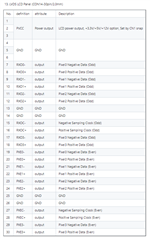
We are working on a prototype automotive infotainment screen for which i would like to convert the parallel short cable from what i believe is 2 Channel 8 Bit with 4 ODD pairs plus ODD clock and 4 EVEN pairs plus EVEN clock.

I have added the pinout for the display below to confirm.

With this in mind is the DS90UB947-Q1EVM and DS90UB948-Q1EVM a suitable evaluation system for achieving this conversion to a single land FPD-LINK III as i would like to use the spare twisted pair in the cable to provide power to the remote screen.

I see on the Evaluation boards there is a microcontroller, is that used for configuring the 947/948 once or is that required for each initialization/power up? This question relates to shrinking the EVM down to a smaller minimal size for placement behind our chosen screens.

Many thanks

Rich
  • Hi Rich,

    Could you possibly clarify on what you are looking to achieve in using the EVMs? Is this for a final system design?

    The EVMs are primarily designed for test purposes only and not necessarily for use in a practical environment, so they are not intended to be modified, including shrinking them down from their existing footprint. 

    The microcontroller is an MSP430 (USB2ANY) which allows for the initialization of each EVM using I2C communication.

    Best,

    Nikolas

  • Hi Nikolas.

    To clarify further, 

    We have an android development kit with the 12.3" screen running over LVDS.

    I want to convert to FPD LINK III . To prove out the design we wish to ensure that the  DS90UB947 and 948 are the correct solution. I assume the easiest way to do this would be to use the EVM kits.

    Once we have a working solution, we would design our own carrier boards including the 947 and 948 along with TI reference design.

    My questions are, 

    1, Based on the datasheet pin out i provided for the screen, is the 947 and 948 a valid solution? resolution is 1920 x 720

    2, Will the 947 and 948 convert to use only 1 pair of HSD twisted cables so that i can use the second pair of twisted cables to supply power from the serializer to the deserializer?

    3, Is the support micro controller necessary for initialization or can the 947/948 be initialized through external setting resistors  (aim is to reduce complexity)

    many thanks
    Rich

  • Hi Rich,

    I want to convert to FPD LINK III . To prove out the design we wish to ensure that the  DS90UB947 and 948 are the correct solution. I assume the easiest way to do this would be to use the EVM kits.

    Thank you for providing this additional context. Yes, in this case, EVMs would be an appropriate solution.

    1, Based on the datasheet pin out i provided for the screen, is the 947 and 948 a valid solution? resolution is 1920 x 720

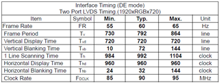
    Yes, from a video timing perspective, the 947 and 948 would be a valid solution, accounting for an approximate 10% of blanking.

    2, Will the 947 and 948 convert to use only 1 pair of HSD twisted cables so that i can use the second pair of twisted cables to supply power from the serializer to the deserializer?

    Just to confirm, you're wondering if, for example, DOUT0 can be used to send data and DOUT1 can be used to send power? Given the above timings, both HSD STP cables would be needed to transmit video data with that PCLK across the FPD-Link on the EVMs, since the device will have to operate in dual link mode to support that PCLK.

    In designing your final system, however, there do exist a variant of HSD connectors, known as "HSD+2," that can transmit the video data in addition to power. This may be something worth exploring if it suits the needs of your system.

    3, Is the support micro controller necessary for initialization or can the 947/948 be initialized through external setting resistors  (aim is to reduce complexity)

    The MSP430 microcontroller is required for initialization to occur, so it should not be removed.

    Let me know if you have any additional questions.

    Best,

    Nikolas

  • Hi Nikolas, 

    Thank you for the reply. That answers most of my questions.

    Regarding the dual mode for timing, the datasheet makes reference to the pixel clock being 90Mhz typical and 95 max, so this should be able to work over just DOUT 0 and not use DOUT 1? or am i wrong?

    The last question in have, the current Android and screen solution using LVDS has dual 4 Data PAirs plus 1 Clock each.

    So in total there are 8 data pairs and 2 clocks coming from the SoM to the Display.

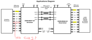
    The 947 only shows 8 data pairs with only ONE clock input, while the 948 shows 8 data lines plus 2 clocks, can you advise where my extra clock for ODD/EVEN should be connected to the Serializer please?

    Thanks
    Rich

  • Hi Rich,

    Regarding the dual mode for timing, the datasheet makes reference to the pixel clock being 90Mhz typical and 95 max, so this should be able to work over just DOUT 0 and not use DOUT 1? or am i wrong?

    Thank you for sharing the table of the timings. Based on the PCLK in this table, you are correct in that the video data could be sent fully in single link mode (over just DOUT0 or just DOUT1).

    The 947 only shows 8 data pairs with only ONE clock input, while the 948 shows 8 data lines plus 2 clocks, can you advise where my extra clock for ODD/EVEN should be connected to the Serializer please?

    The 947 can only accept one LVDS clock input. If you are operating the 947 in DUAL OLDI, both outputs will be timed off one clock input and the OLDI CLK is 1/2 the PCLK (if using dual OLDI). If using single OLDI output, then OLDI CLK = PCLK.

    Best,

    Nikolas