Because of the holidays, TI E2E™ design support forum responses will be delayed from Dec. 25 through Jan. 2. Thank you for your patience.

This thread has been locked.

If you have a related question, please click the "Ask a related question" button in the top right corner. The newly created question will be automatically linked to this question.

SN65HVD12: Output signal not good

Part Number: SN65HVD12
Other Parts Discussed in Thread: THVD1406

Tool/software:

Dear Expert

There is a phenomenon of error code failure in our communication here.
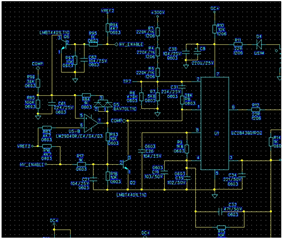
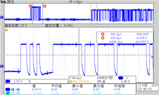
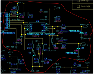
Test signal quality and rise/fall slope. The signal quality from U3 front to isolated IC to chip end is very good (the level voltage and rise/fall slope meet the requirements, less than 2us, impeccable), which means that the signal quality at the output end of U3 backend deteriorates;

The signal quality of RS485_11 is as follows: waveform, falling edge, and slope.
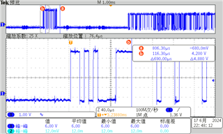

The signal quality of RS485-P1 is good, with the following waveform:
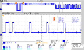
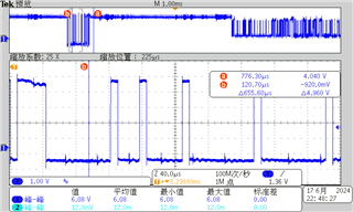
The voltage changes at the two signal terminals are unstable, and the RS485_11 signal has a downward slope, resulting in poor signal quality. Attempted to adjust parameters to optimize but did not see any improvement. Suspect if it is due to chip or USB communication issues? Or it may be due to the coordination of the RS485 communication box, which is currently unclear.

  • That appears to be the wrong part of the schematic.

  • Hi Gabriel,

    1. It appears that you have attached the wrong portion of the schematic - can you please post the RS-485 portion of schematic?

    2. What is the data rate you are running at?

    3. How long is your RS-485 bus? 

    Please let me know.

    Best,

    Parker Dodson

  • Dear Parker

    1.Data rate is 115200;

    2.Line long is 2m.

  • Your circuit controls both the DI and DE inputs from the microcontrollers OUTB output, i.e., when OUTB is high, DE is low. This means that the transceiver actively drives only a low signal; for a high output, the driver is deactivated, and the circuit relies on the fail-safe resistors (R157/R28) to achieve the desired bus voltages.

    With this circuit, slow edges and weaker outputs for high signals are to be expected.

    RS-485 has three states, high, low, and idle. To correctly generate these states, you need to control DI and DE separately. There are some UARTs that can generate the DE signal in hardware; if you do not have such a device, you would need to use a GPIO. Alternatively, use the THVD1406.

  • Hi Gabriel,

    Clemens analysis is correct - in current setup you will most likely have slow rising edges due to the fail-safe network charging the bus for a logic high signal. 

    If you  want auto-direction control- which it appears that you do - there are a couple ways on the RS-485 bus to do it that will actually allow some driving for both high/low states. 

    1. Easiest way to do it is with the THVD1406 - that RS-485 is directly made for Auto-direction with slower signal speeds like your own system. 

    2. We also have an application reference that uses a timer (specifically a 555 timer - it doesn't need to be a 555 timer, it can be any timing IC but the 555 is generally relatively cheap and simple to use) - it will operate similarly to what you have set up now - but it's a little easier to use in practice and setting up your frame length. Essentially the timer starts in the RS-485 device in a "Receive" state then when a transmission occurs on the "D" line (high to low transition) the timer will force the device into transmit mode for the time period that was set up. More details on how to do this can be found here: https://www.ti.com/lit/ug/tidubw6/tidubw6.pdf - please note they do use a different part but this design is applicable to all RS-485 systems, so any standard RS-485 part with enables should be allowed. 

    Please let me know if you have any other questions and I will see what I can do!

    Best,

    Parker Dodson