This thread has been locked.

If you have a related question, please click the "Ask a related question" button in the top right corner. The newly created question will be automatically linked to this question.

DS90UB928Q-Q1: 928 output pattern without FPD LINK cable

Part Number: DS90UB928Q-Q1

Tool/software:

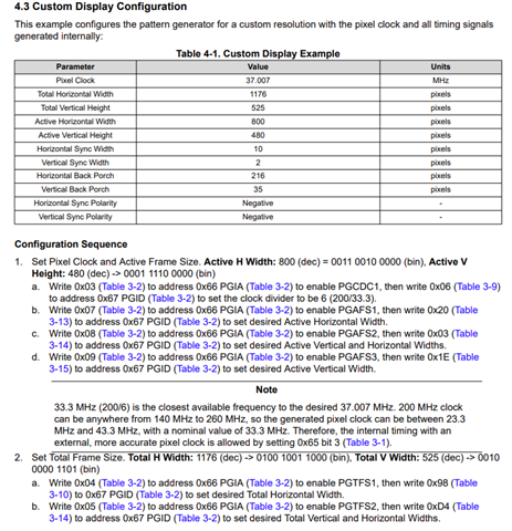
Now we have a project that wants to output the pattern image with 928, but there is no image after configuring the relevant register of 928 through MCU. The display parameter we need is as follows:

The register list we configured for 928 via MCU is shown as below ,(according to SNLA132);

#define PGIA 0X66//!< 间接地址寄存器
#define PGID 0X67//!< 间接数据寄存器

(0X01,0X06);
(0X02,0XF0);
(0X1c,0X03);
(PGIA,0x03);
(PGID,0x05);
(PGIA,0x07);
(PGID,0x56);
(PGIA,0x08);
(PGID,0x03);
(PGIA,0x09);
(PGID,0x1E);
(PGIA,0x04);
(PGID,0xE8);
(PGIA,0x05);
(PGID,0xD3);
(PGIA,0x06);
(PGID,0x20);
(PGIA,0x0C);
(PGID,0x48);
(PGIA,0x0D);
(PGID,0x09);
(PGIA,0x0A);
(PGID,0x06);
(PGIA,0x0B);
(PGID,0x01);
(PGIA,0x0E);
(PGID,0x03);
(0x65,0x04);
(0x39,0x02);
(0x64,0x41);


I2C communication is normal , After configuration, the pattern is not displayed in practice, and the test PLCK is only more than 27MHz, and VS is only 53Hz.However, HFP, HBP and HSW, VSW waveforms are the same as the parameters we set, Please help to check whether there is any configuration we missed or any suggestions. 

  • Hi Bruce,

    The register list we configured for 928 via MCU is shown as below ,(according to SNLA132)

    Which section of SNLA132 are you basing your register configurations off of?

    After configuration, the pattern is not displayed in practice, and the test PLCK is only more than 27MHz, and VS is only 53Hz.However, HFP, HBP and HSW, VSW waveforms are the same as the parameters we set

    Can you clarify on what you mean by "test PCLK is only more than 27MHz"? Do you mean the PCLK is always outputting as 27MHz? Or always slightly more than 27MHz?

    Best,

    Nikolas

  • 1、We configured the registers according to section 4.3 of SNLA132.

    2、always slightly more than 27MHz,but we need 31.5MHz

  • Could you use our configuration to run on the EVM of 928 to verify whether the pattern meeting our 31.5MHz requirements can be generated, or help to check whether our configuration is correct? Thank you

  • Hi Bruce,

    I am working on collecting the necessary hardware to bring-up a 928 EVM set-up, so in the meantime I wanted to corroborate what section of the app note was being referenced.

    In addition, in the meantime, as I work to bring-up a set-up on bench, with regards to the register list provided above, I have some follow-up questions, included below. Note that any lines not explicitly referred to in the above comments look to be correct at first glance.

    • Line 3: Is this a register dump of readbacks or list of register writes? If it is a list of register writes, why is 0x1C being written to? This register only contains read-only status bits.
    • Line 5: The application note writes 0x06 to PGID, but this configuration writes 0x05 to PGID. The current configuration would set the frequency to 40MHz, but writing 0x06 to this register would set the frequency to 33MHz, which is much closer to the desired frequency.
    • Line 27: Confirming that "negative" horizontal and vertical sync widths are desired. 

    The main area of focus right is with regards to line 5 - it looks like the clock divider might be set too high. Are you able to change lines 4 and 5 to the following lines below? This will set the clock divider in such a way that sets the frequency closer to the desired PCLK. Please try this and let me know if this resolves the issue.

    Line 4: (PGIA,0x03);
    Line 5: (PGID,0x06);

    Best,

    Nikolas

  • line 5 ,The internal clock of the 928 is 160MHz, we set it to 0x05, then the clock is 32MHz, we also changed to 0x06, and there also no display

  • Our tests are as follows:
    If the value is set to 0x05, the test CLK output ranges from 27MHz to 28MHz.
    If the value is set to 0x06, the test CLK output ranges from 33MHz to 34MHz.

  • Hello Bruce,

    If the value is set to 0x05, the test CLK output ranges from 27MHz to 28MHz.
    If the value is set to 0x06, the test CLK output ranges from 33MHz to 34MHz.

    I will need to look into these results further. In the meantime, are you able to attempt the programming suggested in "Section 4.2 - Internal Default Timing Configuration" of the SNLA132 app note? This will help identify if the issue is with the custom resolution being programmed.

    Best,

    Nikolas

  • Hello Bruce,

    Are you able to try swapping your sync polarity? Currently, negative sync polarities are being used for HS and VS. Please try flipping the polarity to positive with the programming below and seeing if that brings up the pattern:

    (PGIA,0x0E);
    (PGID,0x00);

    Best,

    Nikolas