Part Number: TLK105L
Other Parts Discussed in Thread: TLK105, AM5728
Tool/software:
Special topic on trial issues
1.1 Background
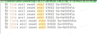
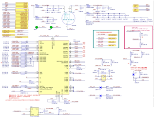
In the test, it is found that the communication control board and serial port expansion board (the same as PCB) will have the problem of no response to the 100 Gigabit network eth3 fault during the temperature change. The principle is as follows: the CPU accesses PHY1/2 through an SMI bus, and the addresses of PHY are 0X01 and 0X03.
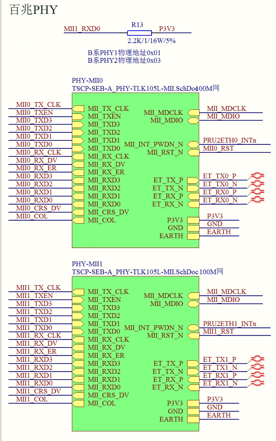
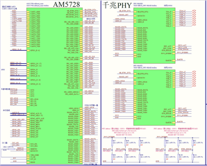
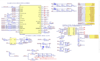
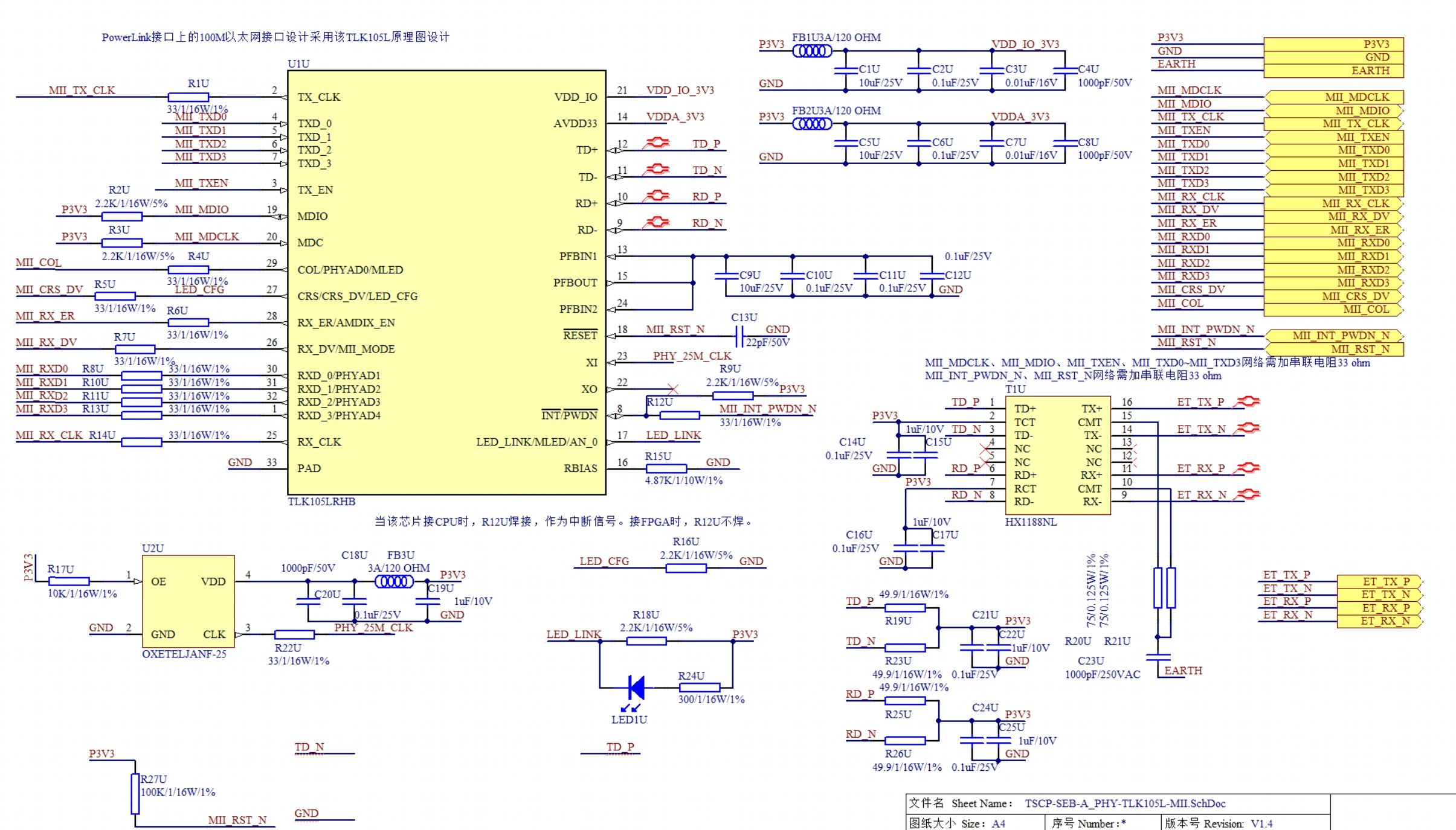
The internal points of PHY are as follows, reusing the schematic of TLK105. But the 83822 has been adapted and the relevant devices on the NC pin of the 83822 have been deleted.
After removing the peripheral device, the three pins are connected by one line, as shown in the following figure:
1.2 Test problem phenomenon
According to the requirements of HASS test, the TSCP host subrack needs to be placed in the HALT test chamber for temperature cycling from -25°C to 60°C, supplemented by vibration. At -20°C, the eth3 network of individual communication control boards is interrupted, and communication cannot be achieved, and ping will also be interrupted.
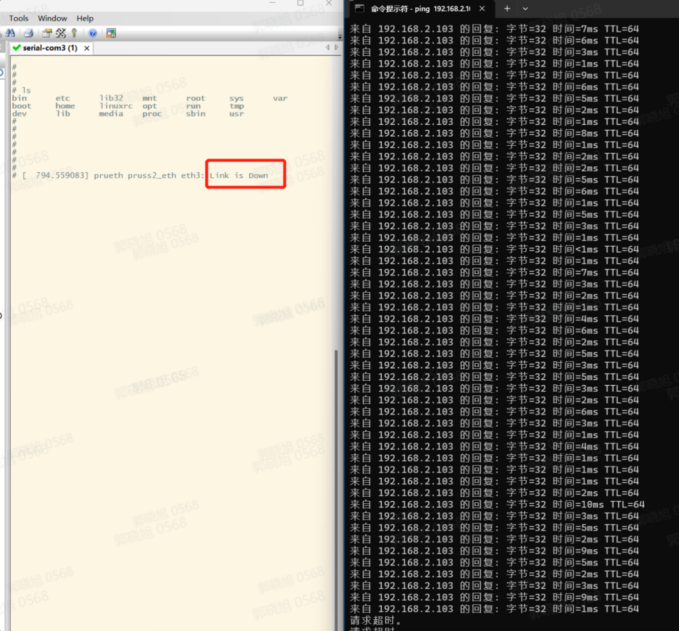
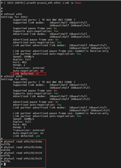
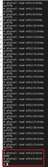
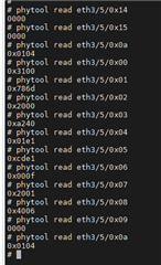
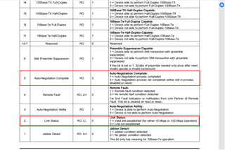
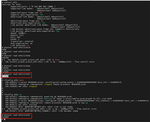
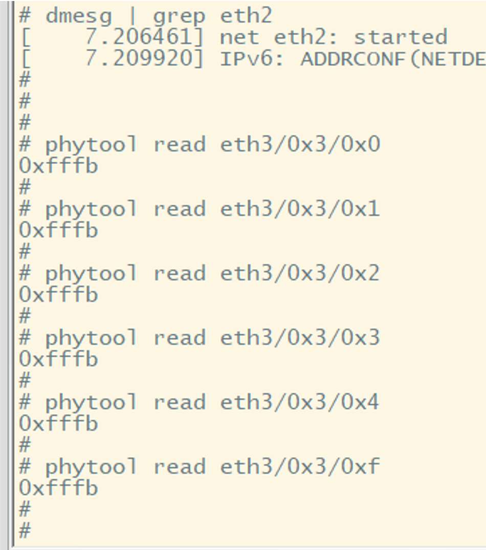
Read the register status of eth3 and find that none of the PHY registers can be read. When the underlying layer of the operating system polls for PHY addresses from 0 to 31, it is found that the PHY address is gone, and any registers for that PHY are inaccessible.
According to the analysis of the problem that TLK105 was replaced with 83822 chip after PHY could not be read at room temperature last year, the phenomenon is consistent with that time.
1.3 Modification adjustment and test verification for problem
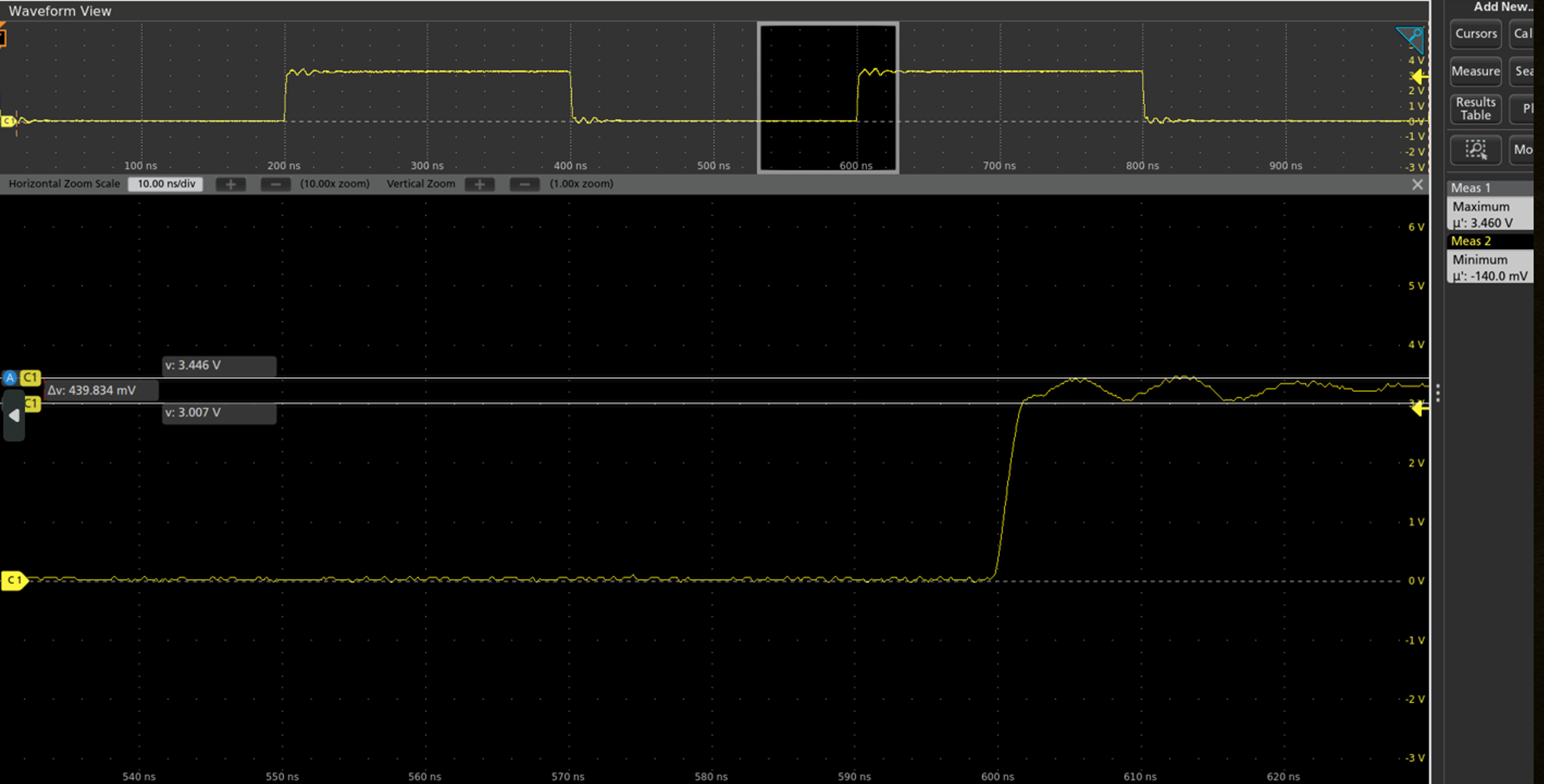
1.3.1 MDC waveform
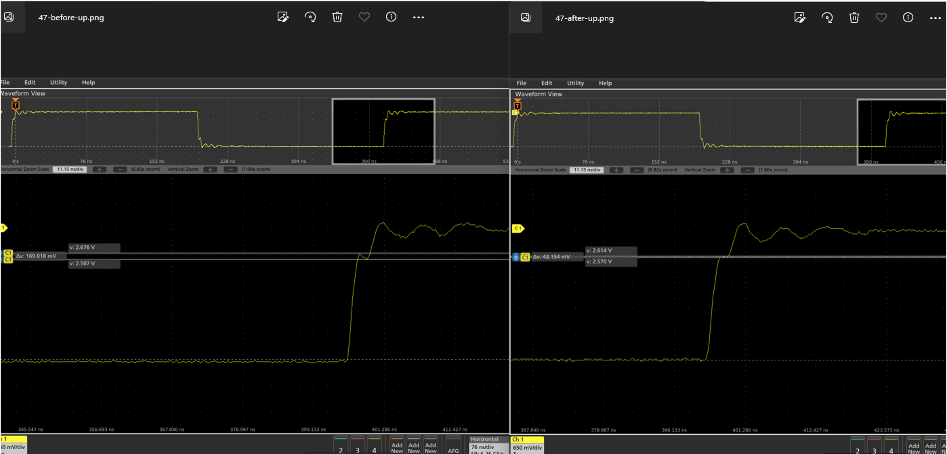
The known scheme can solve the problem of signal interference by modifying MDC and MDIO wiring, but it does not fundamentally solve the source of interference. Therefore, according to the above circuit, the signal test is carried out by adjusting the resistance, the capacitance and inductance of the power supply input and output terminals, and replacing the power supply module. The test record is as follows:
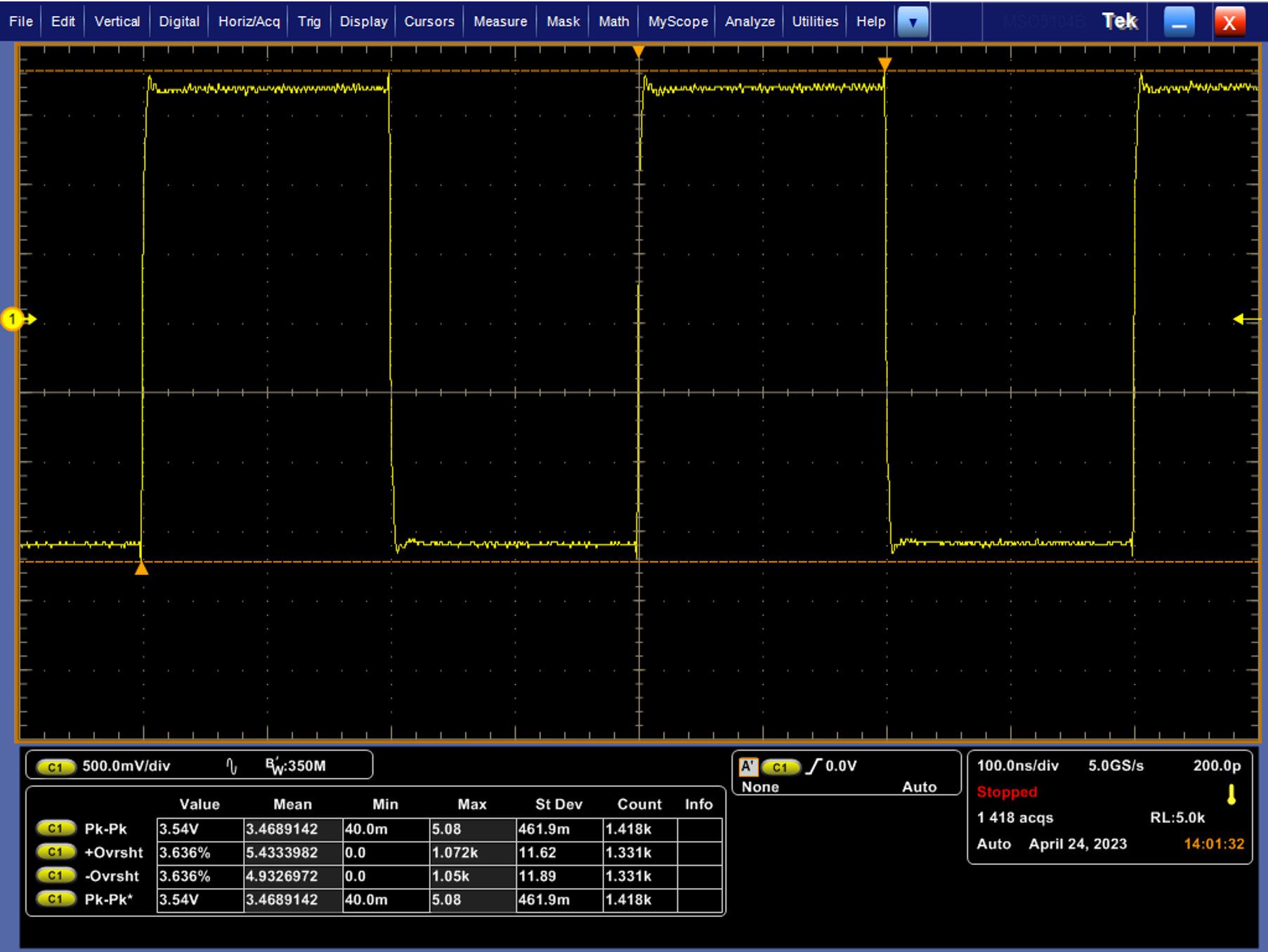
Poor waveform:
Better waveform:
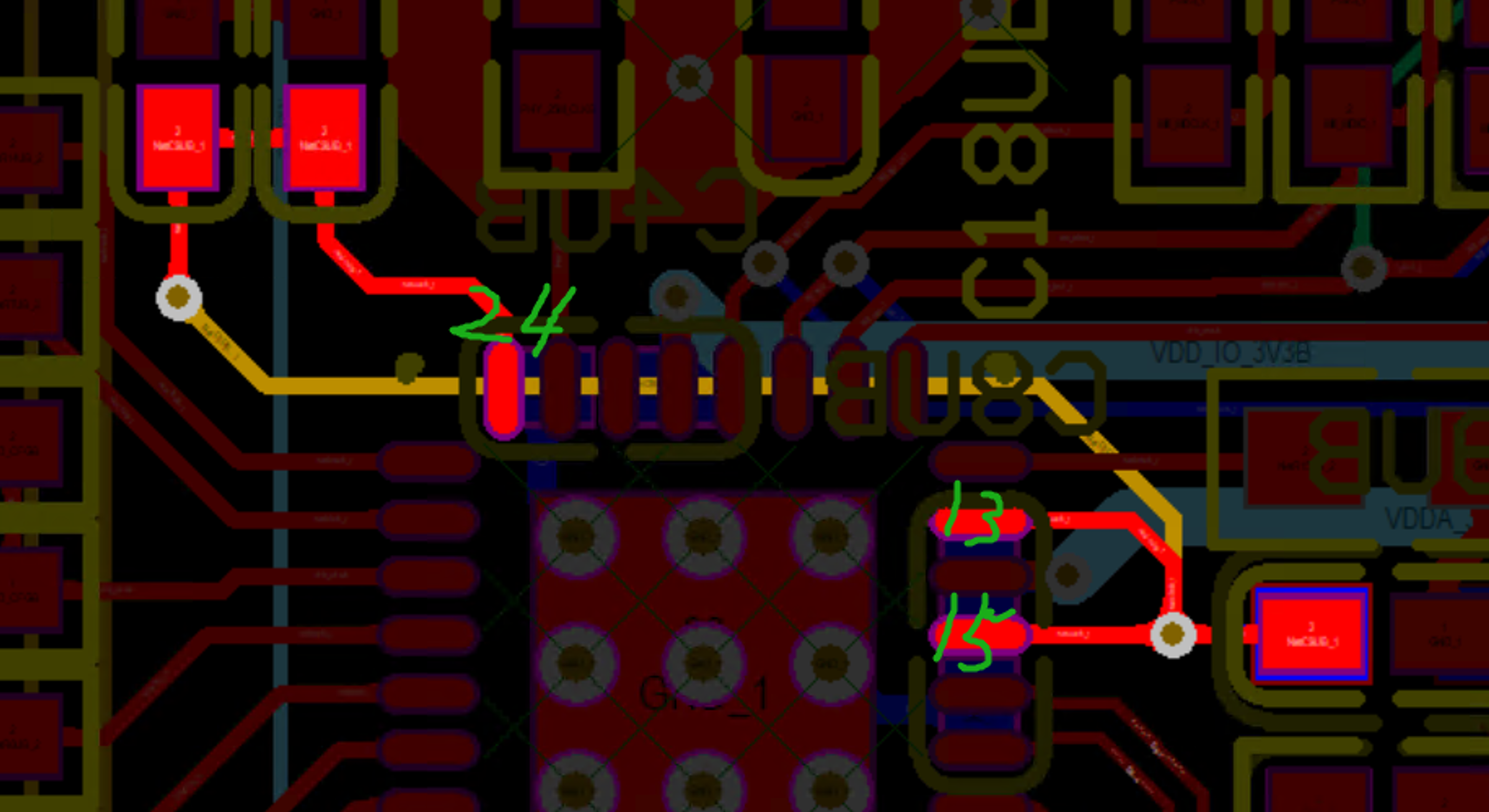
On the basis of this waveform debugging, we have modified a version of PCB, and the modified version has a better test waveform, as shown in the following figure:
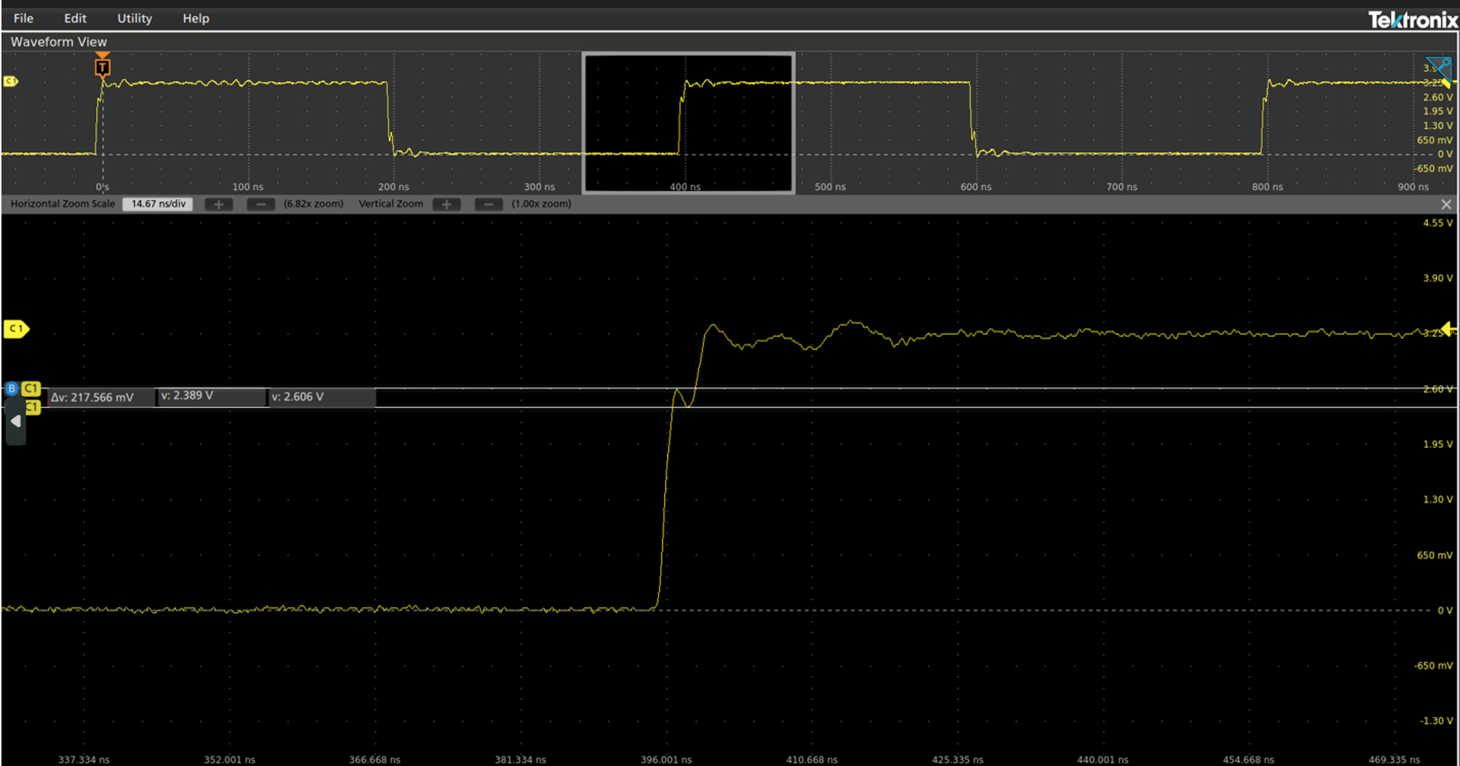
The signal waveform test for SMI bus is as follows:
MDC:
MDIO:
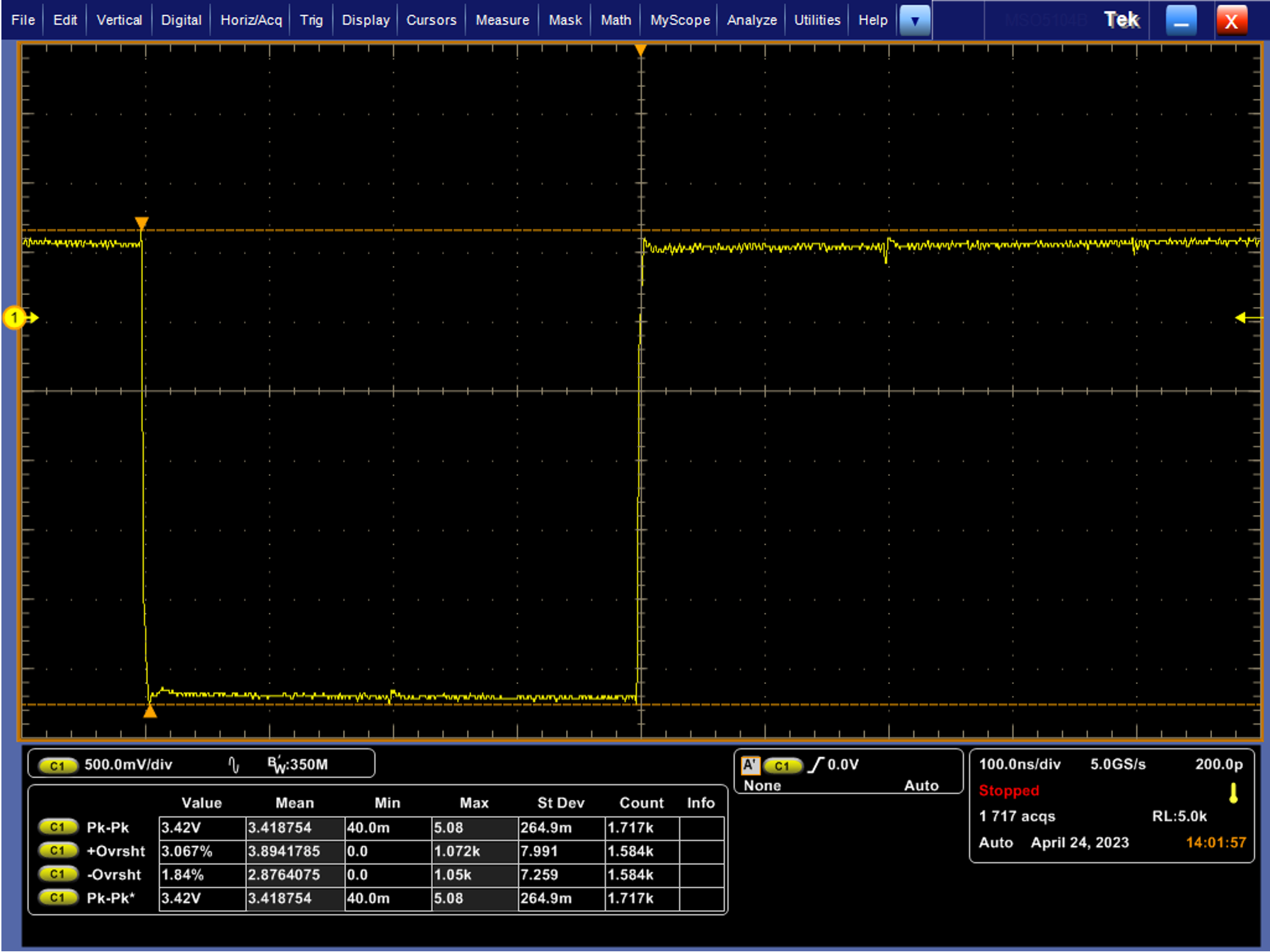
The overall waveform is okay, compared with the multi-capacitor scheme, the MDC overshoot of this waveform is slightly larger by about 1%, but the signal quality is still improved by modifying the wire routing.
And after 500 rounds of testing, there was no problem of PHY disappearing, and the hardware was finalized with this version.
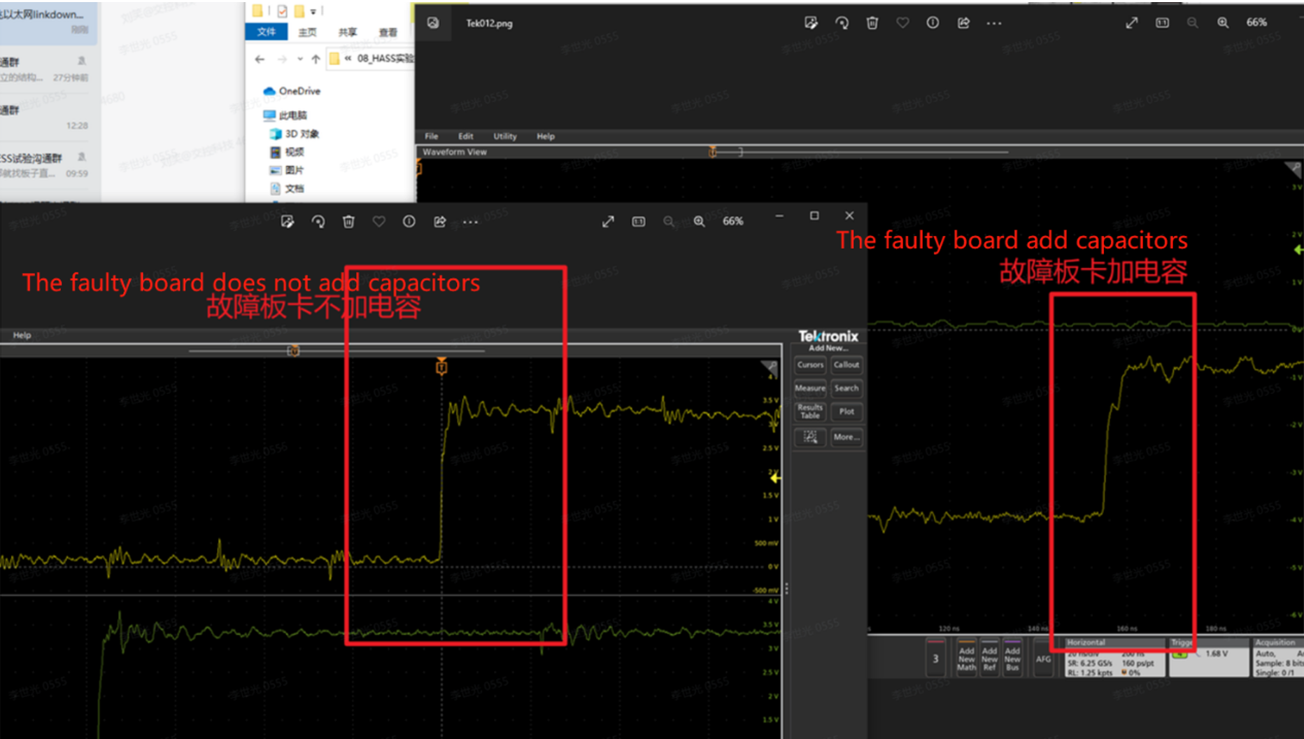
However, similar signal quality problems occurred after our PCB was replaced in common production, and capacitors were added to the MDC/MDIO. But, because the PCB cannot be modified, the capacitor is pulled up to VCCIO, and the test does improve the PHY drop problem of this version of the PCB. The produced boards are rectified according to this plan.
The updated version of the PCB was redrawn according to the pull-down resistor method, and the subsequent board production was carried out.
However, recently, a batch of boards with the pull-up capacitor scheme on the pull-up MDC/MDIO signal line have the problem of PHY disconnection in the aging experiment. The performance of disconnection is the same as before.
At present, the main problem is that it is impossible to confirm what state the PHY is in after it is disconnected and the failure process of PHY cannot be obtained through register access. The network can only be restored to service by the PHY's hard reset signal. What may be the cause of this situation and how to further locate the cause of the failure?