This thread has been locked.

If you have a related question, please click the "Ask a related question" button in the top right corner. The newly created question will be automatically linked to this question.

DS90UB947-Q1: Changing UB947 with external timing mode then UB948 is getting out of lock

Part Number: DS90UB947-Q1

Tool/software:

Hello Team,

The setup is quite simple, UB947 > UB948. Could you please give some advice how to solve this problem?

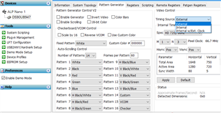
I could generate internal pattern via the following configurations attached. I know the UB948 is locked to UB947 by checking DSUB948_ReadBytes(0x28) and  DSUB948_ReadBytes(0x1C)

Thanks 

Kexiang

the setup could generate internal pattern via the following configurations:

// initialize the page 10 after power up
DSUB947_WriteBytes(0x40,0x10);    	// select OLDI register
DSUB947_WriteBytes(0x41,0x49);    	// force PLL controller in PPM reset state
DSUB947_WriteBytes(0x42,0x16);
DSUB947_WriteBytes(0x41,0x47);    	// force PLL LOCK Low
DSUB947_WriteBytes(0x42,0x20);
DSUB947_WriteBytes(0x42,0xA0);    	// reset PLL divider
DSUB947_WriteBytes(0x42,0x20);
DSUB947_WriteBytes(0x42,0x00);    	// release PLL LOCK control
DSUB947_WriteBytes(0x41,0x49);
DSUB947_WriteBytes(0x42,0x00);    	// release PLL state control

// 2C Control
DSUB947_WriteBytes( 0x03, 0xDA);
DSUB947_WriteBytes( 0x17, 0x9E);

// BRIDGE_CTL
DSUB947_WriteBytes(0x4F, 0xC0);		// Single-pixel mode, OpenLDI mapping

// Gate RGB data with DE
DSUB947_WriteBytes(0x04,0x90);                                   //Prevent AVMUTE for non-HDCP systems

//DUAL_CTL1
DSUB947_WriteBytes(0x5B,0x03);			//Force dual FPD-Link, enable reset on PLL frequency change 

//BCC Watchdog Control
DSUB947_WriteBytes(0x16,0x02);			 //Adjust BCC watchdog timer to minimum 

//GPIO Pass through
DSUB947_WriteBytes(0x0E,0x35);
DSUB947_WriteBytes(0x0F,0x03);
DSUB948_WriteBytes(0x1E,0x53); 
DSUB948_WriteBytes(0x1F,0x05);

// Initialize UB948
DSUB948_WriteBytes(0x4A,0x01); 	 //Disable OLDI outputs on 948 to prevent screen glitches from appearing during the init process
DSUB948_WriteBytes(0x01,0x01); 	 // snapshot reset
//Sleep 100ms

//Initialize SPI Mode
DSUB947_WriteBytes(0x43,0x06); 
DSUB948_WriteBytes(0x43,0x06); 

DSUB948_WriteBytes(0x4A,0x00); // Enable OLDI outputs on UB948

DSUB948_WriteBytes( 0x26, 0x16);
DSUB948_WriteBytes( 0x27, 0x16);

    //PATGEN programming
DSUB947_WriteBytes(0x64, 0x10);          //disabled patttern
DSUB947_WriteBytes(0x66, 0x04);
DSUB947_WriteBytes(0x67, 0x91);
DSUB947_WriteBytes(0x66, 0x05);
DSUB947_WriteBytes(0x67, 0x05);       // h Total = 1425
DSUB947_WriteBytes(0x66, 0x06);
DSUB947_WriteBytes(0x67, 0x31);      // v Total = 784
DSUB947_WriteBytes(0x66, 0x07);
DSUB947_WriteBytes(0x67, 0x00);
DSUB947_WriteBytes(0x66, 0x08);
DSUB947_WriteBytes(0x67, 0x05);      //h Active = 1280 
DSUB947_WriteBytes(0x66, 0x09);
DSUB947_WriteBytes(0x67, 0x30);      //v Active = 768 
DSUB947_WriteBytes(0x66, 0x0a);
DSUB947_WriteBytes(0x67, 0x28);      // h sw = 40
DSUB947_WriteBytes(0x66, 0x0b);
DSUB947_WriteBytes(0x67, 0x02);      //v sw = 2
DSUB947_WriteBytes(0x66, 0x0c);
DSUB947_WriteBytes(0x67, 0x32);      //h bp = 50
DSUB947_WriteBytes(0x66, 0x0d);
DSUB947_WriteBytes(0x67, 0x06);      //v bp = 6
   

DSUB947_WriteBytes(0x66, 0x1a);
DSUB947_WriteBytes(0x67, 0x09);      //M=9
DSUB947_WriteBytes(0x66, 0x03);
DSUB947_WriteBytes(0x67, 0x61);      //N=97 > 74.22     
DSUB947_WriteBytes(0x65, 0x04);      //internal clock and timing
DSUB947_WriteBytes(0x64, 0x05);     // enable colorbar

// Force dual-link mode
DSUB948_WriteBytes(0x34,0x0A);          // PORT1_SEL 
DSUB948_WriteBytes(0x28,0x10);

// Forward SPI channel after RX is locked to TX by checking DSUB948_ReadBytes(I2C_ADDR_DSUB948, 0x1c) 

DSUB947_WriteBytes(0x1E, 0x02);
DSUB947_WriteBytes(0x0F, 0x03);
DSUB947_WriteBytes(0x0E, 0x35);
DSUB947_WriteBytes(0x0D, 0x03); 
DSUB948_WriteBytes(0x34,0x0A);          // PORT1_SEL   
DSUB948_WriteBytes(0x4B,0x02);          // Adjust 0x4B 
DSUB948_WriteBytes(0x1F,0x02);          // GPIO3 
DSUB948_WriteBytes(0x1E,0x02);          // GPIO2-GPIO1         SPCLK MISO   
DSUB948_WriteBytes(0x1D,0x02);          // GPIO0               MOSI
DSUB948_WriteBytes( 0x43, 0x06);       // Forward SPI channel  

//////////////////////////////////////////////////////////////////////////////////////////////
DSUB948 is loss of lock once changed into external timing mode via the step:
DSUB947_Write(0x65, 0x0C); 
//DSUB947_Write(0x65, 0x00);	// default external timing enabled 

  • Hi Kexiang,

    If you have internal patgen with internal timing working then when you switch to external timing mode then you lose lock, there is one of 2 things happening. 

    1. Your external timing or clock is not working as expected from SoC (Video source) 
    2. Or you are switching between these modes on the fly so running one mode then switch to another without full power cycle and re-init (This is not supported) 

    You need to run external mode at power-up you can't switch on the fly from a different mode. 

    Also, which mode are you trying to switch to? External or Internal with external clock?

    Regards,
    Fadi A.

  • Hi Fadi,

    The display functions properly when the video source is directly connected to the panel. I believe such an issue is not related to the video source.

    Firstly, I would like to attempt the mode with an external clock and internal pattern (UB947 reg 0x65 = 0x0c, reg 0x64 = 0x05). I examined that the value read from reg 0x5A is 0x12. It appears that UB947 is operating abnormally. Consequently, UB947 (reg 0x5B = 0x03) is not locked to the external OLDI clock.

    In the case of the internal timing mode, the FPD link always indicates the LOCK during the power off/on of UB948, but the LOCK is always low for the external timing mode.
    Regards,
    Kexiang
  • Hi Fadi,

    Now I have narrowed down the issue with less code. In any case, I have attempted all scenarios, but the external clock fails to function.

    DSUB947_Write(0x40,0x10); // select OLDI register
    DSUB947_Write(0x41,0x49); // force PLL controller in PPM reset state
    DSUB947_Write(0x42,0x16);
    DSUB947_Write(0x41,0x47); // force PLL LOCK Low
    DSUB947_Write(0x42,0x20);
    DSUB947_Write(0x42,0xA0); // reset PLL divider
    DSUB947_Write(0x42,0x20);
    DSUB947_Write(0x42,0x00); // release PLL LOCK control
    DSUB947_Write(0x41,0x49);
    DSUB947_Write(0x42,0x00); // release PLL state control
    delay_ms(10);

    DSUB947_Write(0x65, 0x04); //internal clock OK
    //DSUB947_Write(0x65, 0x0C); //external clock NOK
    DSUB947_Write(0x64, 0x05); // enable patgen

    DSUB947_Write( 0x03, 0xDA);
    DSUB947_Write(0x5B,0x03); //Force dual FPD-Link, disable reset on PLL frequency change
    DSUB947_Write(0x16,0x02); //Adjust BCC watchdog timer to minimum
    DSUB947_Write(0x04,0x90); //Prevent AVMUTE for non-HDCP systems

    do { delay_ms(10); } while ((DSUB948_ReadBytes(I2C_ADDR_DSUB948, 0x1c)&0x13) != 0x13);

    Regards,

    Kexiang

  • Hi Kexiang,

    For internal timing with external clock mode you still need to program the internal timing - Please see example script below. If this doesn't work that mean you have an issue with your SoC clock since this mode uses an external clock to generate the pattern. So if you don't see Lock or video that means your external clock has some issue. 

    #Setting up internal CLK divider to 100Mhz (This only applies to internal timing mode)
    board.WriteI2C(Ser_addr,0x66,0x1A)
    board.WriteI2C(Ser_addr,0x67,0x01) #M=1
    board.WriteI2C(Ser_addr,0x66,0x03)
    board.WriteI2C(Ser_addr,0x67,0x02) #N=2
    
    #Setting up Display Timing based on Customer Panel
    board.WriteI2C(Ser_addr,0x66,0x04)
    board.WriteI2C(Ser_addr,0x67,0x72) #least 8 bit of Total Horizontal frame size
    board.WriteI2C(Ser_addr,0x66,0x05)
    board.WriteI2C(Ser_addr,0x67,0xE6) #Least 4 bit TV + Most 4 bit TH
    board.WriteI2C(Ser_addr,0x66,0x06)
    board.WriteI2C(Ser_addr,0x67,0x31) #Most 8 bit of Total Vertical frame size
    
    board.WriteI2C(Ser_addr,0x66,0x07)
    board.WriteI2C(Ser_addr,0x67,0x00) #least 8 bit of active Horizontal frame size
    board.WriteI2C(Ser_addr,0x66,0x08)
    board.WriteI2C(Ser_addr,0x67,0x05) #Least 4 bit AV + Most 4 bit AH
    board.WriteI2C(Ser_addr,0x66,0x09)
    board.WriteI2C(Ser_addr,0x67,0x30) #Most 8 bit of active Vertical frame size
    
    board.WriteI2C(Ser_addr,0x66,0x0A)
    board.WriteI2C(Ser_addr,0x67,0x28) #Horizontal Sync Width
    board.WriteI2C(Ser_addr,0x66,0x0B)
    board.WriteI2C(Ser_addr,0x67,0x05) #Vertical Sync Width
    board.WriteI2C(Ser_addr,0x66,0x0C)
    board.WriteI2C(Ser_addr,0x67,0xDC) #Horizontal back porch
    board.WriteI2C(Ser_addr,0x66,0x0D)
    board.WriteI2C(Ser_addr,0x67,0x14) #Vertical back porch
    
    #Setting up External Timing with External Clock
    board.WriteI2C(Ser_addr,0x65,0x00) #using External Timing/CLK
    board.WriteI2C(Ser_addr,0x64,0x15) #enable PG/color bars

    Regards,
    Fadi A.

  • Hi Fadi,

    I have identified the reason why external timing fails on the UB947 side. The clock input has not been placed with a 100-ohm resistor. UB948 can be locked to UB947 and is capable of outputting the internal pattern with the external clock.The display shows OK while using external timing and internal pattern. However, a new issue has emerged on the UB947 side. When I modify the mode on UB947 using external timing and data (reg 0x65 = 0x00, by default), the display shows flicker (flashing). It appears that the external LVDS control signals (DE/VS/HS) are not aligne with internal pattern.  Is there any specific format for the LVDS input ?  

    Regards,

    Kexiang

  • Hey Kexiang,

    It appears that the external LVDS control signals (DE/VS/HS) are not aligne with internal pattern.  Is there any specific format for the LVDS input ?  

    No, you shouldn't need to change any settings or format between internal pattern and external CLK mode (0x65 = 0xC0) and external timing/CLK mode (0x65= 0x0) except for register 0x65 value.

    So if you are not seeing an issue with internal timing and external clock mode and seeing HS/VS/DE issue with external timing/CLK mode then this points to a timing issue coming from the video source.

    The only thing you can change is MAPSEL from Mode_Sel1 pin strap or register override. You can also check the filter enable setting in register 0x03 which should be enabled by default.

    However, in MAPSEL issues you will have some discoloration, etc. but in your case with flickering screen/flashing this seems to be a more of a hardware implementation for the data lanes as well to ensure 100 ohm is applied to all lanes and make sure the SoC or video source has a stable video output. 

    MAPSEL register setting

    HS/VS/DE Filter settings

    Regards,
    Fadi A.