Because of the Thanksgiving holiday in the U.S., TI E2E™ design support forum responses may be delayed from November 25 through December 2. Thank you for your patience.

This thread has been locked.

If you have a related question, please click the "Ask a related question" button in the top right corner. The newly created question will be automatically linked to this question.

SN65HVD10: what is the difference between the "13M" and "15M" markings on the SN65HVD10 device.

Part Number: SN65HVD10

Tool/software:

Hi TI Team,

We've encountered communication issues between two FPGA boards using SN65HVD10 transceivers. Specifically, we observed communication breaks when using devices marked "13M." However, replacing them with devices marked "15M" resolved the problem.

Could you please provide insights into the differences between these two markings to understand the root cause of the issue and prevent recurrence?

Thanks

  • The marking should be "VP10". Please show pictures of the actual chips, and tell us whether you bought them from an authorized distributor. Also show us oscilloscope traces of the communication.

  • Hi Vivek,

    As Clemens pointed out, it would probably be best to look at scopeshots of what the issue is and ensure you are buying from authorized distributors. 

    The top markings of TI devices usually have the first line as the device name or a form of the name. The second is the date code and fab site. The last is the lot trace number. 

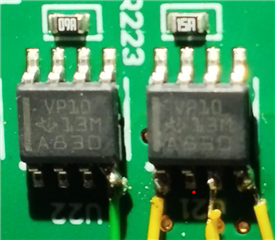
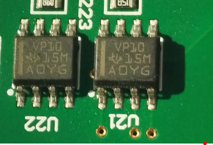
    My guess is the 15M may be 2021 of the month May. And 13M is likely 2021 of March. Assuming the information provided is the second line. Not sure which site the M is but it means they are both from the same fab site.

    -Bobby

  • Hi Clemens,
             yes, i bought from "element14" website.

    meanwhile, below images are shows the devices marked '13M' and '15M'.


  • Hi Bobby,
                  Thanks for your reply.  give me sometime i will attach oscilloscope images.  
    meanwhile, i replied to clemens with images. please look into there for difference of two ICs markings.

    Thanks

  • Hi Vivek,

    Thanks for the picture. 

    I was able to find the lot trace code in our internal database for the 15M marking and it seems to match what we would expect which makes me feel a bit more confident about the part being legitimate. I was also able to locate the 13M device marking as well.

    Are you able to provide a schematic for me to review while we want on scopeshots?

    -Bobby

  • Hi Bobby,
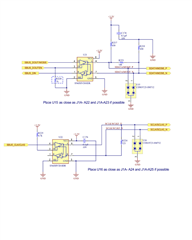
         Thanks for your reply.   below is the schematic image of communication interface FPGA.
    meanwhile, Scope image i will send it soon.


    Thanks

  • Hi Vivek,

    I just checked the schematic. I don't see any major issues. 

    Looks like you have local decoupling, the datasheet pinout matches the schematic pinout, you have termination on both sides/nodes and you included an external failsafe. 

    Only minor thing (doesn't make a difference) is the bottom (U22) device has RE tied to GND but R output is floating. If R is not used, you could tie RE# to Vcc instead to disable the receiver. Again not something that should make a difference or cause a problem (maybe just save some power though).

    -Bobby