This thread has been locked.

If you have a related question, please click the "Ask a related question" button in the top right corner. The newly created question will be automatically linked to this question.

AM26LS31: AM26LS31

Part Number: AM26LS31

Tool/software:

Datasheet link:

AM26LS31 Quadruple Differential Line Driver datasheet (Rev. M)

1) As for 5.8 Typical Characteristics, as the following Figure5-1 and Figure 5-3; both the description of the figure are Output voltage vs Enable G Input Voltage;

but in fact, Vertical axis show the Y output voltage and Output voltage;

I want to know the difference between between Vertical axis show the Y output voltage and Output voltage;(as theFigure5-1 and Figure 5-3 show, the Vertical axis voltage is different)

2) As the Figure5-5, the Vertical axis is High-Level Output Voltage, I want to know the Output Voltage of High-Level Output Voltage is which one of the question 1)?

That means the High-Level Output Voltage is High-Level Output Voltage or High-Level Y Output Voltage

3)Figure 5-9 description is Y output voltage vs Data Input Voltage; Figure 5-14 description is Y output voltage vs Enable G Input Voltage;

       Could you please tell me what is Date Input Voltage and what is Enable G Input Voltage;

  • 1. The Y pin is an output pin. (The graph applies to both Y and Z outputs.) Figure 5-1 shows an output sourcing current; figure 5-3 shows an output sinking current.

    2. As shown by the IOH specification, figure 5-5 shows an output that is sourcing current.

    3. There is no figure 5-14. The input voltage refers to the A pin.

  • Clemens answer is correct.

    1) As for 5.8 Typical Characteristics, as the following Figure5-1 and Figure 5-3; both the description of the figure are Output voltage vs Enable G Input Voltage;

    but in fact, Vertical axis show the Y output voltage and Output voltage;

    I want to know the difference between between Vertical axis show the Y output voltage and Output voltage;(as theFigure5-1 and Figure 5-3 show, the Vertical axis voltage is different)

    5-1 is measuring the VoH of the Y output pin and 5-3 is measuring the VoL of the Y output pin.

    2) As the Figure5-5, the Vertical axis is High-Level Output Voltage, I want to know the Output Voltage of High-Level Output Voltage is which one of the question 1)?

    That means the High-Level Output Voltage is High-Level Output Voltage or High-Level Y Output Voltage

    The output is not shown in 5-5. The VoH in 5-1 is pulling about 7mA of current. (3.3VoH/470ohms=7mA)

    The curve would probably sit slightly above the -20mA curve. 

    3)Figure 5-9 description is Y output voltage vs Data Input Voltage; Figure 5-14 description is Y output voltage vs Enable G Input Voltage;

           Could you please tell me what is Date Input Voltage and what is Enable G Input Voltage;

    5-9 the input is pin A this is just measuring the VoH and VoL of the output pin Y. It doesn't really make sense to track Enable G input unless you care about its V+/V- thresholds.

    -Bobby

  • 1)coud you please tell give the showing test diagram of Load= 470Ω to GND and Load= 470Ω to Vcc, I want to understand it deeper. as the FIgure 5-1 and 5-3showing, on the same VCC supply voltage, the output volge is different. (for example, VCC=2.5V, Figure 5-1 seems 3.5V, but Figure5-3 seems 5.5V); I cannot understand it, coudl you explain?

    2) it is ok for me now

    3) sorry for error input,:

    Figure 5-9 description is Y output voltage vs Data Input Voltage; Figure 5-1 description is Y output voltage vs Enable G Input Voltage;

           Could you please tell me what is Date Input Voltage and what is Enable G Input Voltage;
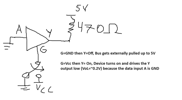
  • 1. There is simply a 470 Ω resistor connected between the output pin (Y or Z) and GND/VCC. In figure 5-1, only the high voltage is generated by the driver; in figure 5-3, only the low voltage is generated by the driver. The other voltage (when the driver is disabled) is determined by the resistor.

    3. When switching the data (A) input pin, the output switches between high and low. When switching the enable (G) input pin, the output switches between the normal level (high or low) and disabled. In figure 5-1, the resistor pulls the output low when disabled (so that you are able to measure the output voltage); in figure 5-9, the output pin generates both high and low voltages, so no load is needed.

  • 1)coud you please tell give the showing test diagram of Load= 470Ω to GND and Load= 470Ω to Vcc, I want to understand it deeper. as the FIgure 5-1 and 5-3showing, on the same VCC supply voltage, the output volge is different. (for example, VCC=2.5V, Figure 5-1 seems 3.5V, but Figure5-3 seems 5.5V); I cannot understand it, coudl you explain?

    The image below is for 5-3. Basically the 5V comes from the external 470 ohm pull up resistor when the device is off/disabled. (This is not what a real RS485/RS422 system looks like). This test is just to test the output strength of Y when it is driving low. The 5V on the graph comes from the external set up where G=GND then the rest of the circuit isn't present/active. It's kind of useless to look at that portion of the graph when G is disabled because it doesn't tell you anything about the device. What matters is when the device is active and driving, that tells you it's drive strength (For x amount of current V equals this, in this case 5V/470 ohms provides ~10mA so VoL at 10mA is about 0.2V of drive or Ron of the NFET is 20 ohms). 

    The set up would be similar in 5-1 but instead the 470 ohm resistor is tied to GND instead. When G is GND, it doesn't matter (that portion of the graph is useless unless you care about the threshold where G switches from Vth- to Vth+). 

      Could you please tell me what is Date Input Voltage and what is Enable G Input Voltage;

    Data input voltage is the voltage at the input defined as the 'A' pin. In figure 5-1 A is held to Vcc and in figure 5-3 A is held to GND. This is what you use to drive the RS485/422 output pins (Y and Z). If A is high, then Y is high and Z is low. If A is low, then Y is low and Z is high. 

    The enable G input just disabled/enables the device. If G is low, the device is basically turned off. If G is high, then A can drive the outputs and the RS485/RS422 bus is now active.

    -Bobby