This thread has been locked.

If you have a related question, please click the "Ask a related question" button in the top right corner. The newly created question will be automatically linked to this question.

DS80PCI102: Please help to review the schematic

Part Number: DS80PCI102

Tool/software:

Hi Support Team,

    There is an 20 inch PCIe 2.0 trace between CPU and NIC in our design, we design to use DS80PCI102 to ensure the signal quality.

    Please can you help to check if there is anything wrong with my schematic ? 


The questions are:

     1. The PCIe2 diff impedance on CPU board is 85ohm that we can't change. Pls help to confirm if DS80PCI102 can support 85ohm for both Tx and Rx path ?

     2. The AC coupling cap on CPU board is 220nF that we can't change. Pls help to confirm if this value is OK for DS80PCI102 on both Tx and RX path ?

Thanks very much !

Tom

  • Hi Tom,

    I'll review your schematic and share feedback by the end of this week.

    The PCIe2 diff impedance on CPU board is 85ohm that we can't change. Pls help to confirm if DS80PCI102 can support 85ohm for both Tx and Rx path

    Yes, 85 ohm differential impedance is within the datasheet specification.

    The AC coupling cap on CPU board is 220nF that we can't change. Pls help to confirm if this value is OK for DS80PCI102 on both Tx and RX path ?

    Yes, 220 nF AC coupling is recommend for PCIe Gen3.

    Best,

    Lucas

  • Hi Lucas,

       About the AC coupling. Pls help check if my understanding is correct or not . Thanks.

      Before: CPU <-> (220nF) <-> NIC

      After:   CPU <-> (220nF) <-> DS80PCI102 <-> (220nF) <-> NIC

    Tom

  • Hi Lucas:

    Add more information based Tom question, This application we use PCIe V2.1 Gen1

    Best Regards

    Lisa

  • Hi Lisa,

    220 nF AC coupling is acceptable for PCIe Gen1 as well.

    Best,

    Lucas

  • Hi Lucas:

    More questions need your help.

    1. For DS80PCI102, How much loss it can sustain/cover? in datasheet it just use length for example, as you know length is impact by PCB material.

    So could you pls share the loss (dB) data for our evaluation?

    2. What location of DS80PCI102 should be placed, in the middle of CPU and I210, or close to CPU, or Close to I210?

    3. in datasheet, Chapter 8.2.1 Design Requirements, it shows

    "For Gen3, AC-coupling capacitors of 220 nF are recommended, maximum body size is 0402, and add cutout
    void on GND plane below the landing pad of the capacitor in order to reduce parasitic capacitance to GND."

    What is the meaning of the sentence marked with Red as above, Can you use a picture to explain?

    4. The Pin as below is also need be used as input when at I2C slave mode, Right?

    4.1 Pin 17: VOD_SEL, VOD should not be modified by I2C command,Right?

    4.2 Pin 18:RXDET, this pin also cannot be modified by I2C command Right?

    and could you explain more about Receiver detect function, I cannot understand just from datasheet

    4.3 Pin 13:RATE, this pin also cannot be modified by I2C command Right?

    And we use Gen 1, How does the IC select or fix the system is Gen 1?

    If tie 1Kohm to GND, it also with de-emphasis or not?

    4.4 Pin 14:SD_TH,this pin also cannot be modified by I2C command Right?

    What is exactly impact if adjust the Threshold?

    Best Regards

    Lisa

  • Hi Lisa,

    1. DS80PCI102 can boost up to 18.4 dB @ 1.25 GHz. This theoretically means 18.4 dB @ 1.25 GHz of insertion loss can be compensated, however there are other factors such as reflections and cross talk which play a role as well.

    2. Since DS80PCI102 is bidirectional, we recommend placing in the middle of CPU and I210.

    3. Assuming high-speed traces are on the top layer, one layer below should be a ground plane. A good layout practice is to cut out the ground plane directly below AC coupling capacitor pads and replace with void. This helps to eliminate noise induction into the component.

    4.1. VOD can be programmed with register settings.

    4.2. While RXDET is controlled by pin setting by default, it can be overridden with register settings.

    When in Auto Rx-Detect, the DS80PCI102 sends small, periodic pulses to sense whether there is a load that is weighing the line down by sinking current through the termination. If the load sinks enough current, the perceived voltage amplitude of the pulses will fall below a pre-determined threshold within the chip so that the DS80PCI102 declares a valid Rx is present, and therefore enables its own internal terminations at the Tx Output.

    When using Manual Rx-Detect, the typical use case is when you know that an endpoint will always be present, particularly in closed systems where the endpoints are predefined and will not be hot-swapped or interchanged at any time during operation.

    4.3. While RATE is controlled by pin setting by default, it can be overridden with register settings.

    1k to GND: This is a limiting mode with de-emphasis intended for Gen 1/2.

    Float: This is a limiting mode with de-emphasis. The redriver detects the number of bit transitions on the incoming signal to determine the data rate/ PCIe Gen.

    20k to GND. This is a linear mode without de-emphasis. Signal path linearity can help facilitate better link training pass through. Although this mode is intended for Gen 3, Gen1/2 can be used in this mode as well.

    4.4. While SD_TH is controlled by pin setting by default, it can be overridden with register settings. This setting is used to change the signal detect assert and de-assert level.

    Best,

    Lucas

  • Hi Lucas:

    Thanks for your kindly explanation.

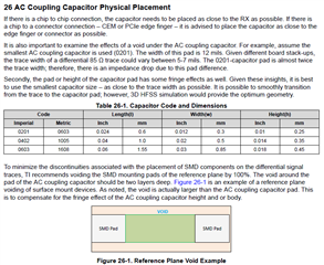
    For question 3: If GND layer void below capacitor , Dose it cause return path discontinuous or long return?

    For question 4.1:Does it mean VOD pin can be NC when we plan to use I2C slave mode?

    For question 4.2: Does it mean RXDET pin can be NC when we plan to use I2C slave mode? or just set to manual RX detect because we are in closed system that CPU and I210 are in one housing and will not be hot swapped.

    For question 4.3&4.4:Does it mean RATE & SD_TH pin can be NC when we plan to use I2C salve mode?\

    Best Regards

    Lisa

  • Hi Lisa,

    Please see this excerpt from app note SNLA426: High-Speed PCB Layout for PCIe Gen 5.

    Keep in mind that VOD, RXDET, RATE, and SD_TH settings will be selected by pin configuration on device power-up. There will be a short period of time before they are changed by register writes. If this won't pose an issue in your system, then I don't see an issue leaving this pins floating. It may still be a good layout practice to include unpopulated pull-up and pull-down resistor pads, so you have the option to change pin settings if needed.

    Manual RX-Detect is likely a good choice in a closed system.

    Best,

    Lucas

  • Hi Lisa,

    Here is my feedback on the schematic. Note that you are still responsible for ensuring that your design will work as intended.

    DS80PCI102_PCIe_Gen1_Schem_Review.pdf

    Best,

    Lucas

  • Hi  Lucas:

    Thanks for your kindly reply and share,

    Best Regards

    Lisa