Part Number: DP83869HM
Tool/software:
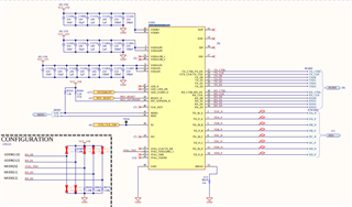
We are using the DP83869HM in the RGMII to Copper configuration and have identified several undesirable conditions related to the boot strapping pin behavior.
Firstly, on the PHY address pins, RX_D0 and RX_D1, we have noticed that the probed voltage on these lines during start up does not correlate to the resistor configuration we have populated. For instance, we have two PHYs and set one of the PHY's address pins to 0xC -- RX_D0 Mode 0 and RX_D1 Mode 3. We set our U-Boot device tree accordingly. However, during boot we are unable to find the PHYs and when the address lines were probed, they read levels that did not align with our resistor configuration.
We then re-arranged the resistor configuration to be Mode 3 for both RX_D0 and RX_D1 -- address 0xF -- and set the address accordingly in the device tree and then we were able to see the PHY populate in U-Boot.
We have a similar board design with this same PHY with the only major difference regarding the bootstrapping pins being that the VDD in that design was 3.3V but is 1.8V in this design. Could the 1.8V VDD be causing these inaccurate voltage levels and therefore misconfigured addresses?
We were then able to communicate with the PHY using MDIO and MII commands in U-Boot but we were unable to establish a connection to our host. Reading from the configuration dump, it appears that AN did not complete for some reason. Moreover, when querying the Bootstrap Status Register 0x6E for PHY A it read 0x30F0. Which correctly corresponds to the RGMII to Copper mode with an address of 0xF. However, it also indicates Port Mirroring is enabled and Link Pass through is disabled. Could this be the reason as to why we were are still unable to communicate with the host?
Here is a copy of our PHY A schematic: