This thread has been locked.

If you have a related question, please click the "Ask a related question" button in the top right corner. The newly created question will be automatically linked to this question.

SN65DSI86: question about SN65DSI86

Part Number: SN65DSI86

Tool/software:

Hello:

Problem:EDP LCD power on timing issue (sleep wake-up jitter)

After continuous sleep and wake-up, it is easy to experience overall screen flickering and jumping, and the positioning and power on timing are not properly adjusted.

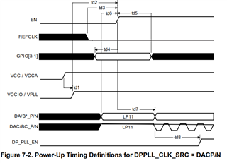
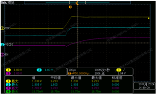
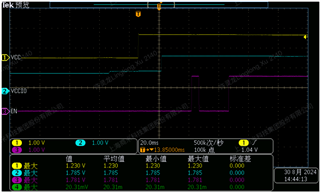
The complete screen power on/off timing diagram is as follows, requiring a certain time difference requirement to be met

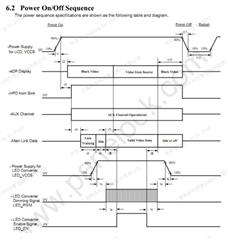
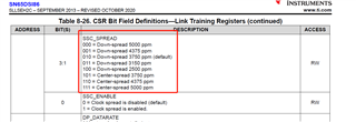
Focus on the signals of the following pins

Power on timing

TXN0 and TXN1 power on first, 3V3 power on later, with an interval of 2.74ms

After 3V3 is powered on, HPD is powered on with an interval of 83.6ms

After HPD is powered on, TXN0 and TXN1 are powered on again with an interval of 361.4ms

Note: TXN0 and TXN1 have a first power on voltage of 0.308V and a second power on voltage of 0.468V

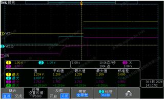
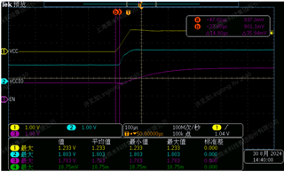
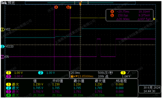
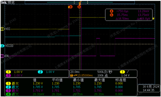
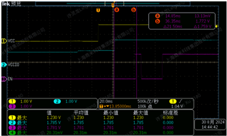
Wake up timing after hibernation

TXN0 and TXN1 power on first, 3V3 power on later, with an interval of 29.8ms, which is much higher than the startup interval of 2.74ms

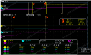
After 3V3 is powered on, TXN0 and TXN1 are powered on again with an interval of 63.44ms

After TXNO is powered on twice, HPD is powered on last with an interval of 28.92ms

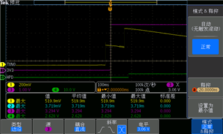
This is the waveform diagram of the wake-up signal from sleep mode

Based on the above test results,

1、there are some issues with TI's output. The EDP timing output by TI chips does not meet the timing requirements of the screen. Among them, TXN0 and TXN1 cannot be controlled by Android. Do you have some suggestion about this timing issue?

2、The customer would like to modify the frequency of the SN65DSI86 chip for verification and requires more explanation and clarification on the frequency expansion

What are the exhibition frequencies here? Percentage or something else

  • Hey Jimmy,

    Can you clarify a few things:

    1) Are you power cycling the DSI86 or the video panel?

    2) Are you following the power on procedure for the DSI86?

    3) The eDP outputs should be AC coupled why do we see them go up to ~0.5V common mode voltage?

    2、The customer would like to modify the frequency of the SN65DSI86 chip for verification and requires more explanation and clarification on the frequency expansion

    What are the exhibition frequencies here? Percentage or something else

    The frequencies here are for SSC clocking where the clock is modulated across a wider range on frequencies to reduce EMI at a single frequency. 

  • Hi Vishesh:

    1) Are you power cycling the DSI86 or the video panel?

    The customer restarted the power supply of the video panel

    2) Are you following the power on procedure for the DSI86?

    1) Both the startup timing and sleep wake-up timing do not comply with SPEC

    2) At present, when testing the input of the Ti chip, it was also found that VCCIO was powered on twice. Android only needs to be powered on once, and it also needs to be checked on the chip side

    Tested waveform when powered on:

    The VCCIO and EN signals are powered on for the first time, with a voltage of approximately 0.96V.

    After 1.652, VCC is powered on first, and then after 14.8us, VCCIO and EN are powered on together. VCC is powered on at 1.2V once, and VCCIO is powered on at the same time

    The second power on voltage of the EN signal is about 1.8V, and the EN pin shows a pull-down and then pull-up signal once.


    Tested sleep wake waveform:

    After turning on, press the shutdown button, VCCIO does not power down, and the voltage is 0.9V. VCC and EN are 0V

    VCCIO is powered on once, and the voltage increases from 0.9V to 1.0V. After 20ms, VCC is powered on, and the voltage increases from 0V to 1.2V.

    After 16.5ms, VCCIO was powered on twice to 1.78V.

    After another 21.5ms, EN will perform power on (1.78V), power off, and power on operations.


    3) The eDP outputs should be AC coupled why do we see them go up to ~0.5V common mode voltage?

    Does it mean that EDP signals cannot be tested with a regular oscilloscope, and high-precision eye diagram oscilloscopes must be used to test high and low level signals of 0 and 1?

    4)The frequencies here are for SSC clocking where the clock is modulated across a wider range on frequencies to reduce EMI at a single frequency. 

    The customer wants to know about the spread frequency and would like to ask how many M correspond to the spread frequency and how the frequency range is calculated?

  • 1) Both the startup timing and sleep wake-up timing do not comply with SPEC

    2) At present, when testing the input of the Ti chip, it was also found that VCCIO was powered on twice. Android only needs to be powered on once, and it also needs to be checked on the chip side

    Is it possible to follow the spec? not following the Spec can put the device in an unknown state. 

    The customer wants to know about the spread frequency and would like to ask how many M correspond to the spread frequency and how the frequency range is calculated?

    This will automatically set by link training. All that needs ot be done is enable SSC and make sure the sink is able to receive an SSC signal.

    Does it mean that EDP signals cannot be tested with a regular oscilloscope, and high-precision eye diagram oscilloscopes must be used to test high and low level signals of 0 and 1?

    Not necessarily, but its odd that the main links have a DC offset when eDP is an Ac coupled interface. Can we try to identify where this jump to 0.468V comes from?

    The customer restarted the power supply of the video panel

    This shouldn't affect the DSI86. Are you able to see stable video when the customer is not power cycling the video panel?

  • Hey,

    I'm closing this thread due to inactivity