


Tool/software:
Hello,
I received some review comments on DS90UB9702 based design. VDD supply decoupling cap, I have used 1uF, 0.1uF and 0.01uF on VDD11xx pin as mentioned in the datasheet and referance design, The reviwer provide some comment on that, Please help to get undersatnd that, basicaly reviwer says in not required.
here is referance schematic part used for review
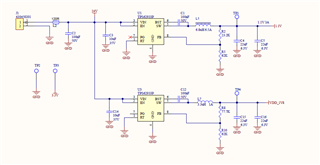
Here is the review comments ans my response.
- 10nF and 100nF in parallel in the same package size has no advantages over just 100nF. Have a look at the measurements of impedance in redexpert, the 10nF don’t have advantages in higher frequencies.my reply:I used 10nF based on the IC datasheet connection diagram ti used 0402 package in the refferance design, I think there will be a technical requiement for 10nF in parrallel with 100nF. eg. internal digital switching speed, probably I/we dont know, I also checked with redexpert, its showing difference of 17MHz/142MHz, may be internal switching frequncy will be in that range, So high frequency may be beyond its usage range. I hope ti will not consider 10nF if it really not required. when I went to the datasheet, I didnt find any technical reason for eliminate 10nFreviwer reply:This setup in datasheets is very common - but with input from Mr. Löckert I started to challenge it. you are right that in this comparison it would make total sense to use 10nF - but 50V is not a realistic voltage for 100nF in 0402. If you compare these with lover voltages like 16V the difference becomes negligible :). The big advantage of eliminating the 10nF is that then there are less parts in the design that have to be close to the IC so the high-frequency routing can be overall optimized - an the bypass capacitors can overall be placed closer to the IC, also lowering the supply impedance the IC seemy reply: I dont see less parts is an advantage over performance. ti should have very specific requirement for 1uF, 0.1 μF, and 0.01 μF capacitors to GND at each VDD pin. other wise they could mention these capacitors are optional. In the data sheet it clearly mentioned as 'Requires'. I would like to add them and if you feel it is really not necessary I suggest to eliminate them while integrating with rcu. second point to added them , may be it is because of internal digital switching noise may be couple to VDD line.reviwer reply:well, less parts and thus a tighter layout can also increase performance, especially if all parts are to be placed on one side of the PCB. If you intent to put the decoupling caps on the bottom like on the layout example this has less impact. Filtering the digital switching noise is all the decoupling caps are about, I try only to make a point on how to minimize this to my experience
- for these extremely low voltages 1uF 0603 parallel to 10uF 0805 does not really make sense as 10uF is also available in 0603with negligible DC biasmy reply: It not parallel in term of placement, there will be series resistance (and 1.1V current is >1.5A) 10uF will be after FB and 1 uF should be close to VDD pin, we dont have much large trace with here, so when on high speed digital switching , trace resiance/impedane will come in to picture. I hvae similar experiance on high speed disign when manufaure placed worng low value capacitance in VDD line, the issue was not even constitant , it occured ramndoly and hard to find simillar issues. issue was solved after replacing the cap.
I aso would like test the perfomance with and without the 0.1uF and 0.01uF, how could I test this?
Thanks
Jolly
