Part Number: TCAN4550-Q1
Other Parts Discussed in Thread: TCAN4550
Tool/software:
Hi Expert,
My customer meet with some questions when they are using the TCAN4550-Q1, please help to answer, thanks in advance
They put 8-byte receive packets in RX0, and more than 8-byte receive packets in RX1, and the diagnostic message is 64 bytes, which is in the RX1.
1. They emulate a few 8-byte packets on CANoe, and then a long packet with a frame cycle of 40ms RX1;
2. Then they send and receive the CAN diagnostic message and find that the response is getting slower and slower, they wonder the reason why TCAN4550-Q1 gets slower and slower;
3. Then they tested and found that if in this case, the long message of 40ms was stopped, the diagnostic message TCAN4550 was no longer reported. It is another issue to resume the transmission of long messages and the diagnostic messages that were not reported will be reported together
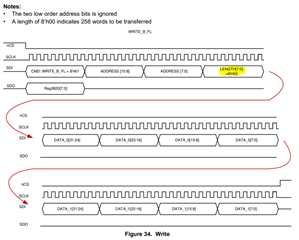
The configuration space is less than 2K, and now the configuration is how many packets are allocated in Rx0 and Rx1.
Best Regards,
Jack