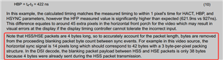
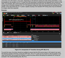
This thread has been locked.

If you have a related question, please click the "Ask a related question" button in the top right corner. The newly created question will be automatically linked to this question.

DS90UB941AS-Q1: What are the DSI source timing requirements for TI941?

Part Number: DS90UB941AS-Q1

Tool/software:

Hi TI:

  When customers use our chip with TI941+TI948, there are a few ics jittering screen, the specific phenomenon is as follows:

  screen timing: pixel clk=147.46MHz, h_act=1920, hfp=64, hbp=32, hsw=32, v_act=1080, vfp=104, vbp=6, vfp=6

  dsi config: 1clock lane+4data lane, dsi clk=445MHz, data rate=890MBps

  About one or two of the 1000 clients will jitter. After measuring the DSI waveform, it is found that the normal chip will enter the LP state for 12 times during one frame, and the abnormal chip will randomly enter the LP state

  for 11 or 12 times. After the dsi data rate is increased to 905MBps, the abnormal IC can also be displayed normally.

  Now we have the following problems to be confirmed by TI:

  1: What causes the above jitter screen?

  2: What is the difference when dsi enter LP state 11times or 12 times during one frame for TI941 parsing timing?

  3: What are the specific requirements of TI941 for the timing of DSI? For example, what are the specific constraints on the dsi clock and timing of the screen for DSI source? How to configure it to ensure the normal display

  • Hi Peifeng,

    Can the information below please be confirmed?

    ==--==--==--==--==--==--==--==--==--==--==--==--==--==--==--==--==--==--==--==--==--==--==--==--==

    1. Video Timing Parameters

      screen timing: pixel clk=147.46MHz, h_act=1920, hfp=64, hbp=32, hsw=32, v_act=1080, vfp=104, vbp=6, vfp=6

    I noticed that the vfp is repeated twice, I am assuming one of these is meant to be vsw?

    With these active and blanking specifications, it looks like total horizontal is = 2048 and total vertical is = 1196

    In this case, with the assumption that the fps is 60, the PCLK should then be 2048 * 1196 * 60 = 146.96 MHz, unless this violates display specifications.

    ==--==--==--==--==--==--==--==--==--==--==--==--==--==--==--==--==--==--==--==--==--==--==--==--==

    2. DSI Mode

    3: What are the specific requirements of TI941 for the timing of DSI?

    This depends on the type of DSI clocking configuration intended for the display, for example there are three types to configure to:

    • DSI Reference Clock Mode
      • This is the most straightforward and commonly used configuration, and the incoming video PCLK is derived from the equation fPCLK = (fDSI*NLanes)/12. More about this in the next section.
    • External Reference Clock Mode
      • Utilizes an external clock on the REFCLK0 or REFCLK1, and it is recommended this is matched to the DSI PCLK. This also follows the equation described above.
    • Internal Reference Clock Mode (typically used for debug purposes only)
      • An internal reference clock utilizes an internal oscillator to generate the output video, but this is typically utilized for debug and self-test mode. 
    What causes the above jitter screen?

    Depending on the mode that is used, jitter could come from the reference clocks incoming to the serializer, but this could also be a marginal case of the frequency not matched precisely to the video timings. Please see next section.

    ==--==--==--==--==--==--==--==--==--==--==--==--==--==--==--==--==--==--==--==--==--==--==--==--==

    3. fDSI

    Given the timing parameters that were shared, it is determined the PCLK should be closer to 146.96 MHz, unless this violates any display specifications (in which case, timing parameters should be updated).

    Using the equation given above, fPCLK = (fDSI*NLanes)/12, then the following calculation should determine the value of fDSI;

    (146.96) = (fDSI)*(4)/(12)

    (146.96)*(3) = (fDSI) = 440.88 MHz or Data Rate of 881.76 Mbps.

    This should be the targeted timing from the Reference Clock if using the two modes

    ==--==--==--==--==--==--==--==--==--==--==--==--==--==--==--==--==--==--==--==--==--==--==--==--==

    The information shared here can also be found within the application note, DS90UB941AS-Q1 DSI Bringup Guide:

    DS90UB941AS-Q1 DSI Bringup Guide (ti.com)

      2: What is the difference when dsi enter LP state 11times or 12 times during one frame for TI941 parsing timing?

    According to MIPI standard, a DSI source should enter Idle Mode (LP-11) or stay in HS mode (LP-00) and transmit the blanking during those times. It is important that the source follows this standard closely, and enters LP-11 during at least of the BLLP periods of the video frame, could you further describe the LP state 11 or 12 that is being recorded between the normal and abnormal?

    Additionally, does increasing the frequency completely remove any jitter? This does not seem to match the other configurations that are used.

    Please let me know your findings and thoughts on this. Thank you!

    Best,

    Miguel

  • ==--==--==--==--==--==--==--==--==--==--==--==--==--==--==--==--==--==--==--==--==--==--==--==--==

    1. Video Timing Parameters

      screen timing: pixel clk=147.46MHz, h_act=1920, hfp=64, hbp=32, hsw=32, v_act=1080, vfp=104, vbp=6, vfp=6

    I noticed that the vfp is repeated twice, I am assuming one of these is meant to be vsw?

    With these active and blanking specifications, it looks like total horizontal is = 2048 and total vertical is = 1196

    In this case, with the assumption that the fps is 60, the PCLK should then be 2048 * 1196 * 60 = 146.96 MHz, unless this violates display specifications.

    A: pixel clk=147.46MHz, h_act=1920, hfp=64, hbp=32, hsw=32, v_act=1080, vfp=104, vbp=8, vsw=8.

        So h_total=2048, v_total=1200, PCLK=2048*1200*60=147.46MHz

    ==--==--==--==--==--==--==--==--==--==--==--==--==--==--==--==--==--==--==--==--==--==--==--==--==

    2. DSI Mode

    3: What are the specific requirements of TI941 for the timing of DSI?

    This depends on the type of DSI clocking configuration intended for the display, for example there are three types to configure to:

    • DSI Reference Clock Mode
      • This is the most straightforward and commonly used configuration, and the incoming video PCLK is derived from the equation fPCLK = (fDSI*NLanes)/12. More about this in the next section.
    • External Reference Clock Mode
      • Utilizes an external clock on the REFCLK0 or REFCLK1, and it is recommended this is matched to the DSI PCLK. This also follows the equation described above.
    • Internal Reference Clock Mode (typically used for debug purposes only)
      • An internal reference clock utilizes an internal oscillator to generate the output video, but this is typically utilized for debug and self-test mode. 
    What causes the above jitter screen?

    Depending on the mode that is used, jitter could come from the reference clocks incoming to the serializer, but this could also be a marginal case of the frequency not matched precisely to the video timings. Please see next section.

    A: We used DSI Reference Clock Mode(sync event pulse)

    ==--==--==--==--==--==--==--==--==--==--==--==--==--==--==--==--==--==--==--==--==--==--==--==--==

    3. fDSI

    Given the timing parameters that were shared, it is determined the PCLK should be closer to 146.96 MHz, unless this violates any display specifications (in which case, timing parameters should be updated).

    Using the equation given above, fPCLK = (fDSI*NLanes)/12, then the following calculation should determine the value of fDSI;

    (146.96) = (fDSI)*(4)/(12)

    (146.96)*(3) = (fDSI) = 440.88 MHz or Data Rate of 881.76 Mbps.

    This should be the targeted timing from the Reference Clock if using the two modes

    A: fPCLK = (fDSI*NLanes)/12 -> fDSI=fPCLK *3

        fDSI=147.46 *3=442.38Mhz or Data Rate of 884.76Mbps

        But 884.76 is not fast enough to transmite pixel data, because we didn't add PACKET HEADER and PACKET FOOTER.

       I see DS90UB941AS-Q1 DSI Bringup Guide (ti.com) 4.3. 

      If we removed HSS/HSE packets from the proceeding blanking packet byte count between sync events the above formula is valid.

      But in MIPI standard I can not found this request, did this request is only TI941 needed?


    ==--==--==--==--==--==--==--==--==--==--==--==--==--==--==--==--==--==--==--==--==--==--==--==--==

    The information shared here can also be found within the application note, DS90UB941AS-Q1 DSI Bringup Guide:

    DS90UB941AS-Q1 DSI Bringup Guide (ti.com)

      2: What is the difference when dsi enter LP state 11times or 12 times during one frame for TI941 parsing timing?

    According to MIPI standard, a DSI source should enter Idle Mode (LP-11) or stay in HS mode (LP-00) and transmit the blanking during those times. It is important that the source follows this standard closely, and enters LP-11 during at least of the BLLP periods of the video frame, could you further describe the LP state 11 or 12 that is being recorded between the normal and abnormal?

    Additionally, does increasing the frequency completely remove any jitter? This does not seem to match the other configurations that are used.

    A:   DS90UB941AS-Q1 DSI Bringup Guide (ti.com) 4.3. 


      Because our DSI Data Rate is 890MBps, so we will enter LP11 in BLLP-4, did this will cause HFP larger than expected?

      Does this means we must ensure that we are in HS mode when transmite a frame of data(each line data not back to LP11). Only  in vertical blanking     area, BLLP-2 back to LP11?

  • Hi Peifeng,

    A: pixel clk=147.46MHz, h_act=1920, hfp=64, hbp=32, hsw=32, v_act=1080, vfp=104, vbp=8, vsw=8.

        So h_total=2048, v_total=1200, PCLK=2048*1200*60=147.46MHz

    A: We used DSI Reference Clock Mode(sync event pulse)

    Thanks for providing this information!

    Does this means we must ensure that we are in HS mode when transmite a frame of data(each line data not back to LP11). Only  in vertical blanking     area

    The suggestion here is to stay in HS during the HFP since it may be longer than expected. LP-11 can be moved within the BLLP as to not disrupt the DSI timing.

    Let's refocus our attention to the potential causes of jitter screen and go through the debug flow that is shown in the application note:

    4.3 Incorrect DSI Packet Timing

    In order to verify the packet timing, and confirm whether this is causing the jitter screen, you may need dedicated DSI analyzer equipment to test the packet timing at the data packet level. We may focus on this later since it requires specialized equipment and analysis.

    If we removed HSS/HSE packets from the proceeding blanking packet byte count between sync events the above formula is valid.

    The horizontal sync start (HSS) and horizontal sync end (HSE) packets are usually included to preserve video timing but are not included in the calculation. They are removed between sync events.

    Since the DSI source is in Event Mode, HSE packets may not be utilized

    ==--==--==--==--==--==--==--==--==--==--==--==--==--==--==--==--==--==--==

    4.4 THS-SKIP Configuration

    For this you may double-check the programmed T-Skip configuration in the 941AS registers. Since there are other units that are working, it may be less likely this is the cause but you may ensure:

    TSKIP_CNT = Round(65*fDSI-5) = Round(65 * 0.442368 - 5) = Round (23.75392) = 24

    • (Note that fDSI is in GHz)

    This will either be on indirect page DSI port 0 (0x40 = 0x04) or port 1 (0x40 = 0x08).

    Depending on which port you are using, configure the indirect register address 0x41 = 0x05 of the DP port (DPHY_SKIP_TIMING Register), set this indirect register value 0x42 = 0x30 (24 in hex is 0x18 -> 0001 1000, but value shifted left 1 bit due to reserved so 0011 0000)

    ==--==--==--==--==--==--==--==--==--==--==--==--==--==--==--==--==--==--==

    4.6 Configuration of Sync Width for Event Mode / Burst Mode

    When the DSI source is configured in Event Mode, you will need to first set DSI_SYNC_PULSES = 0 in the DSI_CONFIG_0 register. This enables override controls for HSYNC and VSYNC, which then DSI_HSW_CFG_HI/DSI_HSW_CFG_LO and DSI_VSW_CFG_HI/DSI_VSW_CFG_LO registers need to be configured. 

    Snice HSW is 32 and VSW is 8, this would then be 0x20 and 0x08 respectively.

    This would then be the following writes to configure the sync width for Event Mode:

    1. Write 0x40 = [0x04 for DSI port 0] or [0x08 for DSI port 1]
    2. Write 0x41 = 0x30 (DSI_HSW_CFG_HI)
    3. Write 0x42 = 0x00
    4. Write 0x41 = 0x31 (DSI_HSW_CFG_LO)
    5. Write 0x42 = 0x20
    6. Write 0x41 = 0x32 (DSI_HSW_CFG_HI)
    7. Write 0x42 = 0x00
    8. Write 0x41 = 0x33 (DSI_HSW_CFG_LO)
    9. Write 0x42 = 0x08

    - - - - - - - - - - - - - - - - - - - - - - - - - - - - - - - - - - - - - - - - - - - - - - - - - - - - - - - - - - - - 

    After confirming these configurations above, if the display still jitters, I suggest taking the clients with jitter screen and run PATGEN from the 941AS-Q1 and see if the screen still displays abnormally. 

    Please let me know if you require additional information running any of the tasks above, thanks!

    Best,

    Miguel