This thread has been locked.

If you have a related question, please click the "Ask a related question" button in the top right corner. The newly created question will be automatically linked to this question.

TLK6002: I am interfacing my TLK6002 with customized FPGA borad, in FPGA board rx clock not getting locked

Part Number: TLK6002

Tool/software:

Hi,

I am transmitting data to TLK6002 board from my customized FPGA board and doing shallow loopback and sendback same data to FPGA borad, in FPGA board sometimes receive clock locking is not happening.

But TLK6002 channel sync happened properly.

While I am configured tx clock, tx data, rx clock & rx data with HSTL logic it is happened but when I configured these signals with LVCMOS rx clock is locking properly.

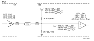
As per my understanding there is no need of termination resistors for LVCMOS logic but in HSTL logic we have to maintain termination resistors.

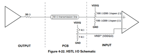
In above figure: Output means TLK6002 generated output impedance?. based on this how much impedance I have to configure in FPGA ip.

From FPGA output how much output impedance I have to provide.

Thanks & Regards,
Mallikarjuna.

  • Hi Mallikarjuna,

    Can you explain what you are changing in your design or configuration when you switch the RXCLK output from HSTL logic to LVCMOS logic?

    50 ohm impedance is internally set on TLK6002 HSTL drivers. 50 ohm impedance still needs to be maintained across the transmission line and at the receiver.

    I have several questions to check if your HSTL logic is configured properly.

    1. Is 50 ohm impedance maintained on all HSTL traces?
    2. Are the RES* pins connected correctly? These are used as a reference for internal terminations on the HSTL inputs and outputs.
    3. Are the VREF* pins connected correctly? These are used as a signal comparison level for HSTL input signals.
    4. Do VDDQA/B power supplies meet datasheet requirements?
    5. Are HSTL electrical characteristics being met?
    6. Are HSTL timing requirements beings met?
    7. Have you tried using all 3 HSTL input termination modes?

    Best,

    Lucas

  • Hi Lucas,

    Can you explain what you are changing in your design or configuration when you switch the RXCLK output from HSTL logic to LVCMOS logic? -> In TLK6002 I was not changed anything for LVCMOS logic, in my FPGA I am considering received signal is LVCMOS and from FPGA I am transmitting LVCMOS logic.

    50 ohm impedance is internally set on TLK6002 HSTL drivers. 50 ohm impedance still needs to be maintained across the transmission line and at the receiver. -> In PCB layout we maintained 50 ohm impedance & at the receiver we kept 50 ohms resistor through FPGA ODT, at this case I am unable to detect rx clock at FPGA ILA.

    1. Is 50 ohm impedance maintained on all HSTL traces? -> Yes
    2. Are the RES* pins connected correctly? These are used as a reference for internal terminations on the HSTL inputs and outputs. -> Yes
    3. Are the VREF* pins connected correctly? These are used as a signal comparison level for HSTL input signals. -> Yes
    4. Do VDDQA/B power supplies meet datasheet requirements? -> Yes
    5. Are HSTL electrical characteristics being met? -> Yes
    6. Are HSTL timing requirements beings met? -> Yes
    7. Have you tried using all 3 HSTL input termination modes? -> Yes

    While transmitting data from FPGA how much output impedance I have to keep in FPGA.

    Thanks & Regards,
    Mallikarjuna.

  • Hi Mallikarjuna,

    Thank you for checking all of my questions. Please set your FPGA output impedance to 50 ohm.

    On your FPGA, what voltage levels are you selecting for HSTL mode and LVCMOS mode? What VDDQ supply voltage are you using on TLK6002?

    Do you have any termination/resistor network design on the FPGA HSTL receiver?

    Best,

    Lucas

  • Hi Lucas,

    Please set your FPGA output impedance to 50 ohm -> FPGA output impedance selected 48 ohm, by using FPGA output impedance selection, no physical circuits are available.

    On your FPGA, what voltage levels are you selecting for HSTL mode and LVCMOS mode? What VDDQ supply voltage are you using on TLK6002? -> voltage levels for HSTL & LVCMOS as 1.8V and VDDQ as 1.2V

    Do you have any termination/resistor network design on the FPGA HSTL receiver? -> We dont have any termination network design on the FPGA HSTL receiver, we can select input impedance using FPGA.

    Thanks & Regards,
    Mallikarjuna.

  • Hi Mallikarjuna,

    48 ohm output impedance should be sufficient.

    VDDQ needs to be 1.5V or 1.8V. Can you try supplying 1.8V so it matches your FPGA voltage mode?

    Best,

    Lucas

  • Hi Lucas,

    We are supplying VDDQ as 1.8V, In my previous reply I gave wrong info, sorry for that.

    Thanks & Regards,
    Mallikarjuna.

  • Hi Mallikarjuna,

    I understand, thank you for the clarification.

    When you select HSTL mode on your FPGA, does the internal termination on the receiver look like this?

    When you select LVCMOS mode, is there any internal termination? I'd like to understand what is changing on the receiver end between the 2 modes.

    Best,

    Lucas