Part Number: TMUXHS4446
Tool/software:
Hello,
I have a non-traditional application that needs to support DP in and DP out over a single USB-C connector.
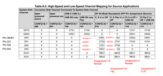
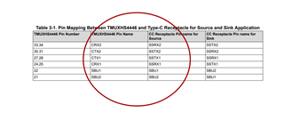
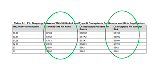
My mux architecture involves the TMUXHS4446, but I would like to clarify how the connector-side pins connect to the system-side and DP pins. I saw that Table 6-3 and Table 6-4 give the pinouts based on if the mux is being used in a source or sink application. Since I'm not strictly following a source or sink application, I'm not sure how to interpret the table. From what I can tell, there is no way to tell the part it is in source or sink, so TI is trying to simplify the design by showing how to connect the pins to the connector to line up the DP lanes and USB signals.
What I would really like is a table that shows which pin numbers are connected for each of the CONF[2:0] modes.
For example, if CONFG[2:0] = 010, does pin 39 (DP0+) connect to either pin 34 (CRX2+, source) or pin 31 (CTX2+, sink)?
Thanks,
Ryan