Part Number: SN75LVDS83B
Tool/software:
Hi,
we have built a process control board with an HMI interface and we are now testing it.
For the 800x600 pixel TFT display that we have to manage, we have provided both an RGB and LVDS interface. The latter is obtained with the SN75LVDS83BDGG component connected as reported in the attached electric diagram.
LVDS MP106 Rel 030124.pdf
The RGB display works perfectly (we have been using it for years) while the LVDS one does not (this is the first time we have used it).
By investigating with oscilloscope, datasheets, forums, etc. we immediately saw an high ripple on the LVDSVCC power supply which we eliminated by short-circuiting the two choke filters L15 and L16.
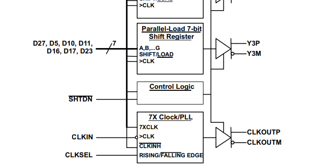
After we saw that of the 5 pairs of differential LVDS signals the CLKOUT one does not move, while the other 4 do.
Both CLKOUT signals are still whether connected to the LVDS display or to a simple 100 Ohm resistor.
On the CLKIN signal there is the 40 MHz clock signal generated by the graphics controller and the /SHTDN pin is off (3.3 V).
After 2 days of research we have not found any explanations and for this we decided to write this request.
Can you help us? Any suggestions are welcome.
Thanks in advance and best regards.
Gianluca Angelini
Software department