This thread has been locked.

If you have a related question, please click the "Ask a related question" button in the top right corner. The newly created question will be automatically linked to this question.

DS90UH948-Q1: LVDS fan-out in Repeater mode

Part Number: DS90UH948-Q1
Other Parts Discussed in Thread: LMK1D2102

Tool/software:

Hello, 

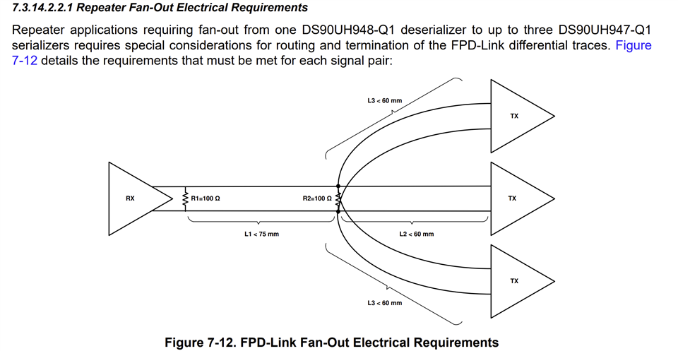
We are designing device which should implement HDCP repeater mode according to Figure 7-12, p.38 in datasheet. But concerning about signal integrity issues in such configuration. To check this we performed simple simulation for setup/configuration from Figure 7-12, and got quite bad results even at low LVDS speeds (100 - 200MHz for single LVDS pair). While point-to-point setup works quite well. We used DS90UH947 at the receiver side.
The question is: will HDCP repeater configuration work, if we insert fan-out buffer between DS90UH948 and DS90UH947? Something like LMK1D2102 or similar.

Best regards, Aleksandr

  • Hi Aleksandr, 

    As advertised in datasheet, fanning out one OLDI output to multiple inputs is technically possible, but has some technical challenges in signal integrity, termination, impedance balancing, etc.

    100 - 200MHz for single LVDS pair

    Single OLDI output only supports up to 96MHz 

    Is HDCP authentication being targeted, or only fanning out to multiple transmitters with repeater?

    If single OLDI port is being targeted, you might consider using Replicate mode to generate a secondary "clone" of single OLDI data, which can be routed point to point to next 947.

    Furthermore, 947 also has a TX replicate mode; where when combined with above - you can get 3 total duplications with only 2 947 SERs without any "fan-out".

    Regards,

    Logan

  • Hello Logan, 

    thanks for reply

    To clarify a bit my questions and your points:

    - the target application is fanning out to multiple transmitters, namely - remote displays

    - we target to dual OLDI output and dual FPD Link In and Out ports

    - to be honest I thought that OLDI data lanes run at 7x faster frequency that clock lane. Having 96 MHz clock we will get 672 MHz on data lanes. Taking maximum 196 MHz Open LDI clock frequency in dual link we will get 1372 MHz on data lanes. Correct me if I'm wrong


    - since datasheet states: "In addition to providing the video data, the LVDS interface communicates control information and packetized audio data". We are wondering if 948 communicates somehow with downstream 947 devices? And inserted fan-out buffer will  corrupt this communication?

    Best regards, Aleksandr

  • Hi Aleksandr, 

    To avoid any misunderstanding, can you provide a block diagram of what you are looking to achieve? Are you intending to fan-out to other SERs to retransmit FPD-Link to another module or send to OLDI receivers (displays, etc)?

    - to be honest I thought that OLDI data lanes run at 7x faster frequency that clock lane. Having 96 MHz clock we will get 672 MHz on data lanes. Taking maximum 196 MHz Open LDI clock frequency in dual link we will get 1372 MHz on data lanes. Correct me if I'm wrong

    PCLK frequency is 1/3.5 that of OLDI data frequency.

    Regards, 

    Logan

  • Hello Logan,

    Are you intending to fan-out to other SERs to retransmit FPD-Link to another module or send to OLDI receivers (displays, etc)?

    we intend to fan-out to other SERs

    below is block diagram we currently have, with LVDS lanes simply connected together:


    and what we expect to be when we insert LVDS fan-out buffer to split LVDS lanes:


    blocks named "LVDS Display" are outside of this device. They shown so it will be clearer what on the higher level

    Best regards, Aleksandr

  • Hi Aleksandr, 

    Thanks for the clarification - much more clear now. 

    The first diagram should be possible, provided that the SI is okay and the input jitter on OLDI CLK satisfies the input requirements of final 3 SERs. 

    My concern with the second approach would be the skew/jitter requirements of 947 CLK/data inputs might be violated when passing CLK/data through these fan-out buffers. While it would make the fanning out/termination more straight-forward, very careful consideration and checks would be needed to validate. 

    Regards, 

    Logan

  • Hello Logan, 

    Thanks for the answer.


    Can you please clarify what is allowable skew for 947's OLDI CLK/Data lanes. Haven't find this info clearly described in datasheet 

    Best regards, Aleksandr

  • Hi Aleksandr, 

    Please find attached. 

    Regards, 

    Logan7268.947 Jitter and Skew Measurements.xlsx

  • Hello Logan, 

    Thank you for the calculation of jitter and skew, and for measurement notes. Will try to check it in our system 

    Best regards, Aleksandr