Part Number: DP83826I
Other Parts Discussed in Thread: TPS22965,
Tool/software:
Hi Team,
TPS6521902 has been used as shown in SLVUCL0 Figure 2-3 with an external FET switch of type TPS22965 to switch through the P3V3_VSYS voltage.
By testing the parts, it was noticed that the PMIC turns on the FET switch, but then the DVDD1V8 rail of the processor, which is generated via Buck2 of the PMIC, is not turned on. With an oscillator, it was measured the following voltage curve:

Channel 1 is connected to P3V3_VSYS (voltage at the output of the power switch TPS22965), channel 2 is connected to the DVDD1V8 rail of the processor (generated by Buck 2).
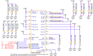
The voltage seen on channel 2 is output via the two PHYs DP83826I on the DVDD1V8 rail.
These are connected (each via a dedicated ferrite) on the VDDA3V3 rail to P3V3_VSYS voltage (= output TPS22965) and to your VDDIO rail to the DVDD1V8 rail (= buck 2 of the PMIC).
When the ferrites from the VDDA3V3 rail of the PHYs are triggered, the PMIC starts up normally.
The assumption is that the PMIC does not start up, because the voltage on channel 2 is approx. 0.8 V above the PMIC's "short circuit (SCG) and residual voltage detection (RV) low-going threshold" of 220 mV to 300 mV.
Is the acceptance correct?
Can you understand the behavior of the DP83826I or has something been overlooked here?
Since the plan is to operate the PHY with an I/O voltage of 1.8 V, one option could be to connect another power switch to the VDDA3V3 rail of the PHY, whose enable input is connected to the DVD1V8 rail (= buck 2 of the PMIC).
What do you think about it?
Regards,
Marcela