This thread has been locked.

If you have a related question, please click the "Ask a related question" button in the top right corner. The newly created question will be automatically linked to this question.

TIC12400-Q1: abnormal at ADC input mode

Part Number: TIC12400-Q1
Other Parts Discussed in Thread: TIC12400, , TIC10024-Q1

Tool/software:

Hi team, 

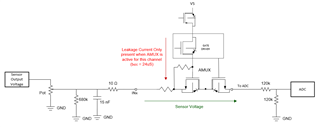
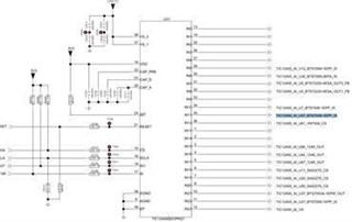
We met a problem on using ADC input mode of TIC12400. The input of IN11 is analog signal. You can find the circuit of input side as below. 

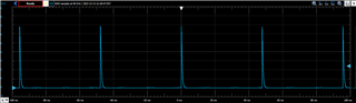
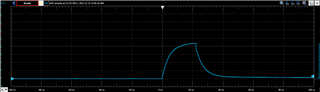
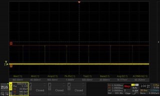
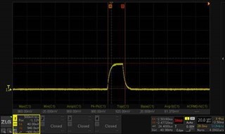
They are using ADC polling mode, the wetting current is configured to 0mA. But they captured an abnormal periodic pulse at IN11. You can find the waveform as below. 


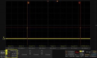
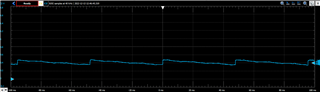
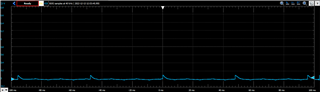
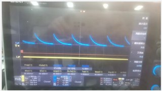
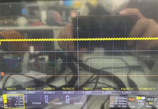
I suspect that it is cause by IIN_LEAK_0mA. After placing a 15nF cap at IN11, the voltage level get worse, see below. Please help provide some suggestions to debug. 
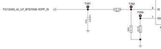
Schematic as below. 


Thanks!

Ethan Wen

  • Hello Ethan,

    You are correct, this is due to the leakage current with 0mA (+/- 110uA max).  I'll explain the issue with the following example.

    The leakage current comes from the Analog MUX pass FET gate bias circuit that is used to connect the enabled INx channels to the ADC for measurement one at a time.  This leakage current is only active on an INx channel when the MUX is actively connecting it to the ADC which is typically 24uS and specified as tADC in the datasheet.  This is essentially equivalent to enabling a pullup resistor to VS that is between 100k-200k in value for 24us when the measurement is being made.  Typically this is absorbed with the current source or sink current when it is a non-zero value.

    There is also a resistor divider on the input to the ADC that steps down the voltage to a safe level that is within the ADC range.  The total input resistance is specified as 240k, which means that each resistor is essentially 120k.  This too is only connected to the INx pin during the moment of measurement, but this is in parallel with external restive loads to GND during the moment of measurement.

    Typically there is a low pass filter on the INx pin for ESD protection that includes a series resistor and shunt capacitor and therefore an equivalent circuit would look something like the following figure.


    The voltage measured by the ADC will depend on the external components connected to the INx pin.  With a completely open pin (i.e. with no filter components) the only path for the leakage current to flow is through the internal resistor divider at the input to the ADC.  During this time, the ADC will see a voltage that is greater than the 6V max ADC code 1023 (0x3FF)

    When there is a capacitor added to the INx pin (such as with the ESD filter), the capacitor will charge for 24us while the MUX is actively connecting it to the ADC, and discharge for the remaining duration of the polling cycle.  Without any pulldown resistance or other voltage source to charge/discharge the cap, the capacitor will only discharge through parasitic resistance on the board and may not reach a completely discharged state.  This results in some DC offset voltage and is dependent on the capacitor value, and the polling cycle time.  The following scope is from adding a 15nF cap to same board from the previous measurement.  Note there is a 48ms polling cycle time for this test.  This cap reduces the pulse amplitude to 130mV peak-to-peak, but established a 0.4V common mode voltage.  The ADC returned a value of 89 (0x59)

    Adding an external 100k pulldown resistor to the INx pin provides a discharge path to remove the common mode voltage and further reduces the leakage current pulse amplitude.  The ADC now returns a code of 20 (0x14).

    Zooming in on a pulse shows the pulse duration correlates to the tADC spec time in the datasheet that is typically 24us.

    The initial observations provided of an ADC value between 29-31 is consistent with my example data, but with slightly different circuit components that result in slightly different ADC values.

    So, to your question, you will need a capacitor to absorb (decouple) this leakage current, and some form of discharge resistance to prevent the cap from establishing some DC offset. I hope this helps you understand how the device is working.

    Regards,

    Jonathan

  • Hi Jonathan, 

    Thanks for your detailed explanation. 

    Based on your suggestions, customer tried 22nF capacitor and below combination at the input of IN11, the result is acceptable. 

    But they have some requirements for the response time of this analog input signal, which mean the RC value should not such high. If C=22nf, they prefer to use R2=470ohm. Considering some corner cases that analog input voltage may reach 12V in short time. Do you think 470ohm resistor is enough for current limiting protection? 

    We also want to change R1 to 10ohm. Do you think increase the R1 value will also help on reducing the leakage impact? 

    Regards,

    Ethan Wen

  • Hi Ethan,

    Yes, I think 470 ohm should be more than enough, perhaps even more than is needed.  I would refer you to the TIC12400-Q1 and TIC10024-Q1 ISO-10605 ESD Test Report (Link) for more information about the RC Filter components and what levels of ESD protection they can provide to help with the determination of what components the customer wants to use for their application.

    The ESD Ratings table in the datasheet uses 15nF and 33 ohms for the power-ed up +/-8kV rating.

    Regards,

    Jonathan

  • Hi Jonathan, 

    Thank you! It is clear. 

    Besides, customer observed some abnormal at digital input mode as well. See the waveform and schematic as below. 

    Why and how to fix it? 

    Regards,

    Ethan Wen

  • Hi Ethan,

    Please provide more details about the device and register configuration so I have a better understanding about how the device is operating which will allow me to better understand the waveforms.

    However, I believe this is just the leakage current, that I previously explained, charging the filter cap when the device is making the measurement.  The cap is then discharging through the very large resistance made up of 100k + 3.3k resistance to GND. 

    The 100k series resistor is very large for these applications?  Why have they chosen such a large value?  I would suggest using a lower value resistor which will allow the cap to discharge the leakage current more quickly.

    Regards,

    Jonathan

  • Hi Jonathan,

    Let me get the register configuration and get back to you later. 

    This is not the same case with we talked previous in this thread. This abnormal comes from digital input mode. Does the leakage also have in digital input mode? 

    Thanks!

    Ethan Wen

  • Hi Ethan,

    I don't know what you the "digital input mode" is since this isn't language in the datasheet.

    The device can be configured to "source" wetting current (CSO) or "sink" wetting current (CSI).  It can also be configured to "continuously" source/sink this current, or to periodically enable the wetting current during the measurement and then disable it for the remainder of each "polling" cycle.  The device also have an ADC or Comparator that can be used to make the voltage measurement and determine the switch state. 

    Because the comparator can only provide information about whether the INx pin's voltage was above or below the threshold, it is sometimes referred to as digital when compared to the ADC that can provide an actual code between 0 and 1023 that can represent exactly what the voltage is and is therefore considered "analog".  But it will be helpful to only use the terms of the datasheet to avoid confusion.

    Having the register configuration will be verify helpful.

    Thanks,

    Jonathan