Because of the Thanksgiving holiday in the U.S., TI E2E™ design support forum responses may be delayed from November 25 through December 2. Thank you for your patience.

TCA9617B: Using B side on common bus of star topology?

Part Number: TCA9617B
Other Parts Discussed in Thread: PCA9306, LSF0102, , LSF0002

Tool/software:

I have a case where I need an I2C star topology translator. One slave bus must be set to 1.8V. The other slave bus is user-selectable between 1.8V and 5V. The master bus voltage is flexible. (See diagram)


The TCA9167B almost works except the requirement that the A-side has to be on the common side of the star topology. If I use that topology, the B-side voltage doesn’t support down to a 1.8V bus. So I’m wondering, can I run a star topology with the B-side on the common bus? I realize that the one 9617 on the bus won’t see the low logic driven from the other 9617, but does the I2C bus still function properly? Is the concern that the inactive slaves could see erroneous clock/data that causes them to misbehave? Why can't the B side be used on the common bus other than the logic level drive/threshold limitation?

Another option is to run VccB at 2.2V with pull-ups to 1.8V. This should still meet the logic high threshold (ie 0.7 * 2.2V = 1.53V), but I’m concerned that it will be difficult to run at 1MHz given that the logic high is near the top end of the RC time constant.

If this topology doesn’t work, can anyone suggest an architecture that would? I need FM+ with one I2C bus at 1.8V and another I2C bus at a user-selectable voltage between 1.8V and 5V.

Thanks,
Ned

  • The LSF0102/PCA9306 allows flexible voltages on both sides, but it not a buffer.

  • Hi Ned,

    Connecting B-sides of two TCA9617B is not allowed. This results in oscillation. See app note

    This connection would only work if you are able to control each TCA9617B via its EN pin. Only allow one TCA9617B to be enabled at any given time. 

    The TCA9617B is only rated for 2.2V to 5.5V on B-side. Using the device at 1.8V on B-side is outside datasheet spec. 

    Do you need buffering due to high cap loads on the bus? Clemens has suggested level translating alternatives if only level translation is needed. 

    Regards,

    Tyler

  • Thanks Clemens. I believe the 9306 will work, but I believe it requires a "step down" conversion to a dummy bus because the 9306 looks to require Vref2>Vref1. Because my master bus can only go down to 1.8V and my user-selectable bus is required to support 1.8V, I believe my only option is to run multiple 9306's with 1.2V as an intermediate bus voltage (see diagram). Can you provide any feedback on this approach? Much appreciated!

  • You do not need three translators. The only restriction of the PCA9306 is that the I/O voltages must not be lower than VREF1. With VREF1 = 1.8 V and VRFEF2 = any higher voltage, you can use any pull-up voltage between 1.8 V and 5 V on any I/O pin.

  • Hi Ned,

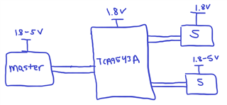
    In addition to Clemens' comments here, have you looked into using an I2C switch? 

    The TCA9543A might work well here.


    Regards,

    Tyler

  • Tyler and Clemens, thank you both for the help. I am working with Ned on this design and we are trying to maintain FM+ 1Mhz speeds. It looks like the switch part you show only goes to 400kHz.  

  • I appreciate your input, but I'm not sure I follow. There appears to be a criteria that VREF2 >= VREF1 + 0.6V. So if I run VREF1 = 1.8V, then VREF2 >= 2.4V. I don't understand how the pull-up voltage on the VREF2 side can still be at 1.8V? Are you implying that 1.8V still meets the logic high threshold of 0.7*VREF2=1.68V? My concern with that is can it still operate at FM+ (1MHz) speeds given how close the threshold is to the pull-up?

  • Hi Tyler, we have considered a switch, but would prefer to avoid it to avoid additional complexity. In my mind, a switch or the three PCA9306 option I discussed above are our best options.

  • Hi Ned & Bryan,

    Tyler and Clemens, thank you both for the help. I am working with Ned on this design and we are trying to maintain FM+ 1Mhz speeds. It looks like the switch part you show only goes to 400kHz.  

    You are correct. I missed the note about FM+. 

    I appreciate your input, but I'm not sure I follow. There appears to be a criteria that VREF2 >= VREF1 + 0.6V. So if I run VREF1 = 1.8V, then VREF2 >= 2.4V. I don't understand how the pull-up voltage on the VREF2 side can still be at 1.8V? Are you implying that 1.8V still meets the logic high threshold of 0.7*VREF2=1.68V? My concern with that is can it still operate at FM+ (1MHz) speeds given how close the threshold is to the pull-up?

    What Clemens is suggesting is that as long as the IO voltage (SCL1/SDA1/SCL2/SDA2) is > VREF1 = 1.8V, you can select any voltage higher than 1.8V... (2.5V, 3.3V, 5.0V) as the pull-up voltage regardless of VREF2. 

    For example...

    VREF1 = 1.8V

    VREF2 = 2.5V

    SCL1/SDA1/SCL2/SDA2 = 1.8V <--> 5V 

    The only electronic component that connects side 1 to side 2 is a passFET internal to the PCA9306. As long as the EN voltage (gate voltage) of the transistor is set correctly, the pull-up voltages on side 1 or side 2 can be set to 1.8V - 5V if VREF1 = 1.8V. 

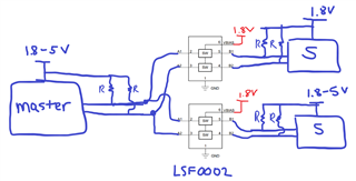
    I ran this design past another engineer on my team. Have you looked into LSF0002? I think this might be the cheapest solution I can find for y'all. 

    LSF0002

    Regards,

    Tyler

  • That makes sense. I think we have a solid approach to our I2C bus. Thanks Tyler & Clemens!