Because of the Thanksgiving holiday in the U.S., TI E2E™ design support forum responses may be delayed from November 25 through December 2. Thank you for your patience.

DS34LV87T: The output P during idle time will have a strange waveform

Part Number: DS34LV87T

Tool/software:

Hi sir,

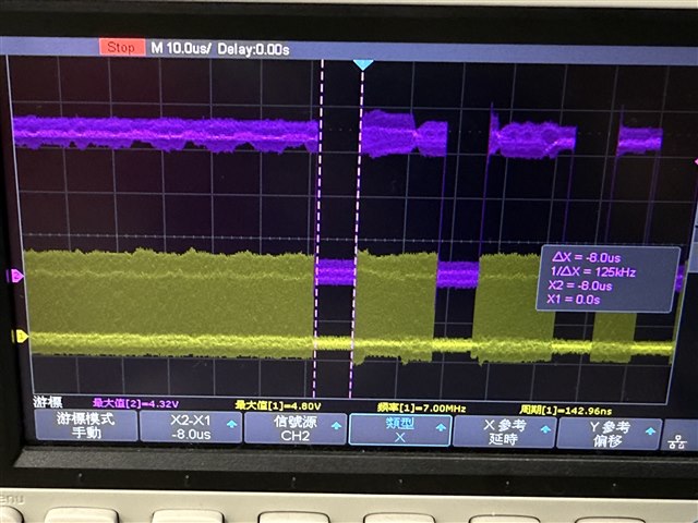
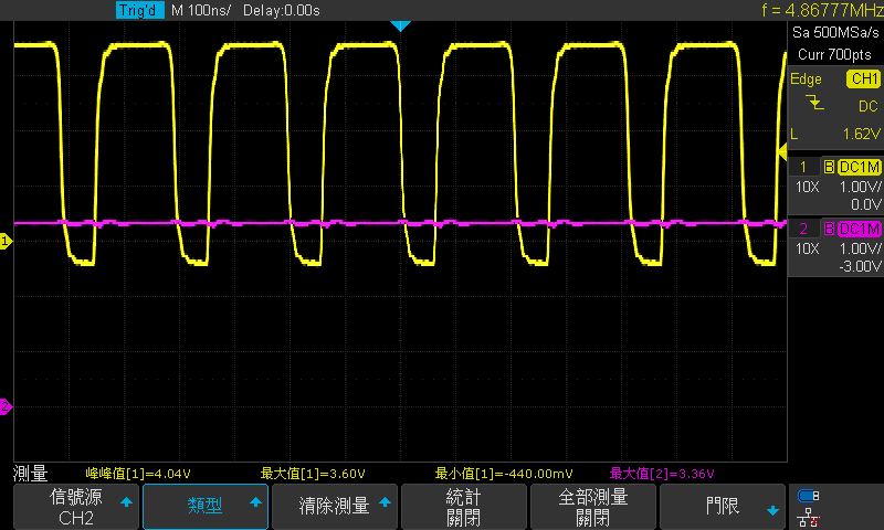
Our system uses three DS34LV87T chips to convert the UART signal from single-ended to differential. Currently, we are encountering a problem where the output P exhibits the waveform shown in the image below when there is no input signal connected.(only pull-up)

All three ICs are experiencing the same issue. We have attempted to add termination resistors 100 Ohm to the output to prevent it from being left floating, but this has not resolved the issue.

The output N does not produce any waveform.

However, strangely, this state still allows for normal transmission of the UART signal.

  • Hi Vincent,

    Thank you for sharing all of that information. I have several questions and suggestions for you:

    • Could you share a scope image at the input pins while this oscillation is happening on the output? I wonder if there is a chance the pullup resistors to VCC are interfering.
    • Do all 4 output P lines (output+) show this waveform? 
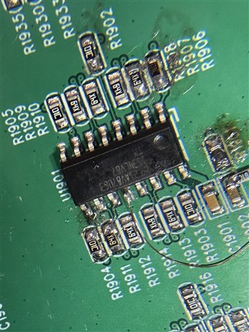
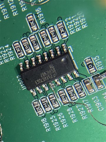
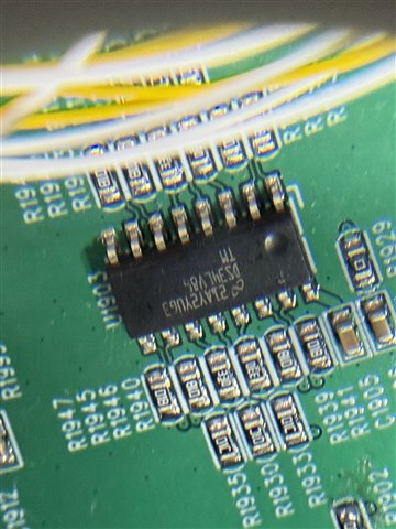
    • Can you send a picture of the top of the device? I want to confirm these devices are legitimate as sometimes counterfeit devices enter the market through third parties. 

    Regards,

    Ethan

  • Hi Ethan

    Let me revise my statement: the UART reception is abnormal.

    1. We have tried removing the pull-up resistors and physically lifting the input pins, but there has been no change in the output signal.
    2. Currently, all three components in my possession are exhibiting the same condition, including those with only the "TP (test point)" reserved, which also show the same waveform.
    3. Below are the photos of these three components.


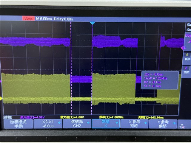
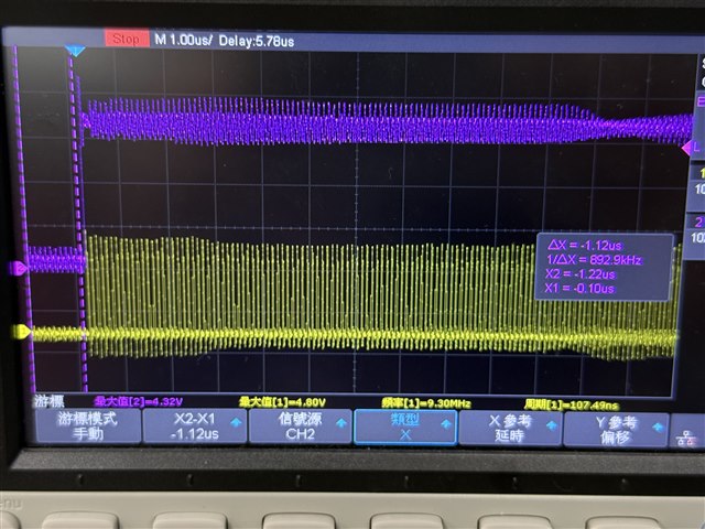
    Additionally, here is the waveform while transmitting a UART signal (CH2 in purple is the input; CH1 in yellow is the output P). When the UART input is low, output P is also low; when the UART input is high, the output displays an abnormal signal (the dashed line marks one bit of data).

  • Vincent, 

    Thank you for those additional details. I have looked into those specific devices, and they all appear legitimate on my end. 

    Here are a couple more questions:

    • Is it possible there are high frequency emissions close to where these devices are operating?
    • Could you send a waveform of the receiving end of the signal? Is it possible the source is down the line coming from the receiver?
    • Can you share a full system schematic? 

    The reason I ask for a schematic is that I do not see any ESD protection diodes for those devices. It is possible that these devices experienced ESD strikes above their rated protection. We recommend placing ESD diodes on the bus lines, particularly the ESDS552.  

    Regards,

    Ethan

  • Hi Ethan,

    • There are no high-speed signals or signals above 50 MHz nearby.
    • At the receiving end, as shown in the previous response with CH2 (purple), when the receiving end receives HIGH, the output P will also be HIGH, but it will exhibit a strange waveform. We have tried disconnecting the source and testing solely with the DS34LV87 IC, and the results show that as long as the receiving end is HIGH, the output end will also be an abnormal HIGH.

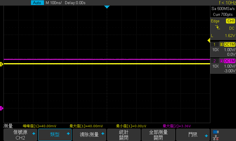
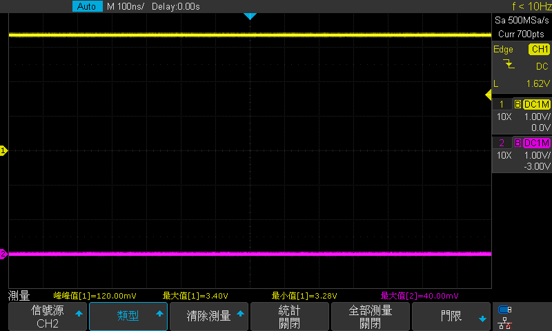
    CH1: output +; Ch2: intput set to High

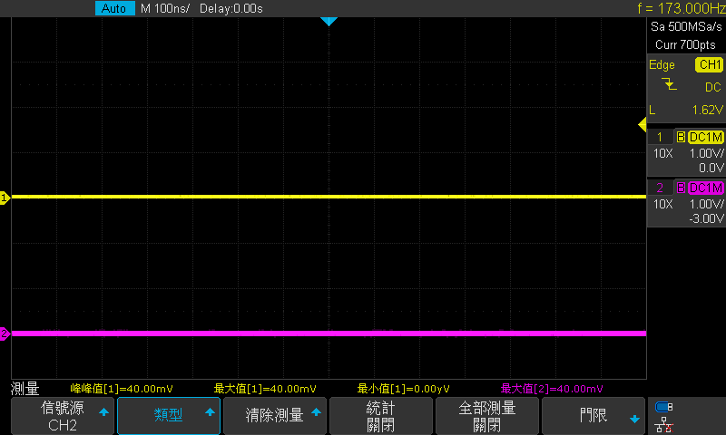
    CH1: output +; Ch2: intput set to Low

    CH1: output -; Ch2: intput set to High

    CH1: output -; Ch2: intput set to Low

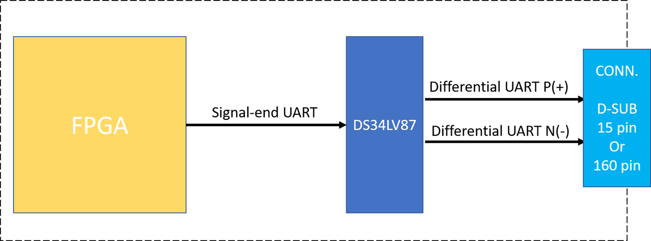
    • Due to confidentiality issues, we may not be able to provide complete information, but we can provide a block diagram.

    The FPGA is directly connected to the input of the DS34LV87.

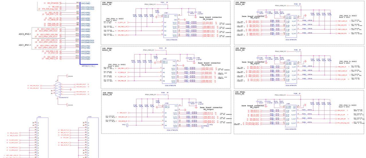
    All DS34LV87T are all connected to the connector. (I only show some of the conn side.)

    In our design, there are no ESD-related circuits.

    Vincent

  • Hi Vincent, 

    Could you reupload those images? They are not showing up for me. 

    My biggest concern is that the devices might have been damaged since ESD protection was not implement into the design. However, if you are concerned that this is a device failure that you did not cause, you could send a device to us using our Failure Analysis process: https://www.ti.com/support-quality/additional-information/failure-analysis.html

    I will show this to my colleagues for a second opinion. 

    Best,

    Ethan 

  • Hi Ethan,

    I reupload the images as below,

    The datasheet shows the ESD protection value as ESD ≧ 7kV. I don't think it is that fragile. If ESD had damaged three DS34LV87Ts, it wouldn't be reasonable for all three of my DS34LV86Ts to be normal.

    • There are no high-speed signals or signals above 50 MHz nearby.
    • At the receiving end, as shown in the previous response with CH2 (purple), when the receiving end receives HIGH, the output P will also be HIGH, but it will exhibit a strange waveform. We have tried disconnecting the source and testing solely with the DS34LV87 IC, and the results show that as long as the receiving end is HIGH, the output end will also be an abnormal HIGH.

    CH1: output +; Ch2: intput set to High

    CH1: output +; Ch2: intput set to Low

    CH1: output -; Ch2: intput set to High

    CH1: output -; Ch2: intput set to Low

    • Due to confidentiality issues, we may not be able to provide complete information, but we can provide a block diagram.

    The FPGA is directly connected to the input of the DS34LV87.

    All DS34LV87T are all connected to the connector. (I only show some of the conn side.)

    Vincent

  • Hi Ethan,

    Update on the current situation: We have tried adding a 33-ohm resistor between the damping resistor at the output and the P and N of the IC (we tested resistors from 45 to 100 ohms, but not all of them worked correctly for each channel). At this point, P can output a normal waveform and can be received.

    However, in this state, my P/N output voltage in the high state drops from 2.1V to 2.3V, showing a significant voltage drop. Additionally, after adding 12 sets of 33-ohm resistors, my system has noticeably increased power consumption by 1.5W.

    Vincent

  • Hi Vincent,

    Thanks for all of the updated information.

    I might be confused on one part if you could clarify: are the N outputs outputting a normal waveform as well? Or is only the P outputting a waveform as you mentioned in your last message? 

    Based on your testing of the 33 Ohm resistor, I believe the oscillation you were seeing is a reflection issue. Now that I can see the receiver schematics, there is a clear termination issue that is causing this reflection. This document further explains why proper termination is necessary ( it details RS-485 but the same reasoning applies).

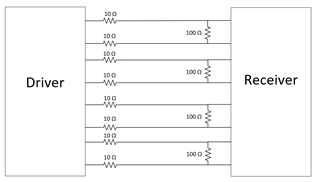
    In your schematic, there is 45 Ohms in series with the driver lines and 1K Ohms in series with the receiver lines. In typical RS-422 setups, these should be completely removed or replaced with 10 Ohm resistors pulse proof resistors (for transient protection). This is help to properly match the characteristic impedance of the lines.

    Ideally, a 80 to 100 Ohm termination resistor should be placed connecting each positive and negative input of the receiver only (resistor from A_IN- to A_IN+ and so on). The driver should not have any termination resistors (this helps with EMI and it best practice for minimizing reflections). So similar to your 33 Ohm testing, there should be 12 of these in total. The tradeoff here is yes the output voltage will drop, but signal integrity will be greatly improved. The power consumption will increase with added termination resistors as you indicated, but considering there are 12 drivers in total that increase is actually rather good. In general RS-422 is not known for being low power. 

    One last point: I still highly recommend adding ESD protection to the bus lines. Yes, the device has 7kV Human Body Model (HBM), but for comparison industrial rated designs typically have up to 30kV IEC ESD protection (more rigorous protection than HBM standard). It is not that device is that fragile, more so that the environment surrounding it can be quite prone to ESD strikes.

    Regards,

    Ethan

  • Hi Ethan,

    Thank your reply.

    I have reworked the DS34LV87 with the following circuit, keeping only the connections to the IC, so there are no reflection issues. The presence or absence of the pull-up resistor at the input does not affect the output of the strange signal.

    I attempted to pull the input high or low for testing, and the results are as follows:

    under this setup with 100 Ohm, output P still sends strange waveform when the input is High signal.

    When the input is H, it will exhibit a strange waveform; when it is L, the output will be a normal L.

    Whether the input is H or L, the output is normal (input L results in output H; input H results in output L).

    This is what I mentioned: only the output P exhibits an abnormal waveform, while the output N does not.

    So the output of the DS34LV87 is connected to a device or left floating, the output P will be abnormal when the input is high.

    So your suggestion is to modify the DS34LV87 like this?

    However, for the termination resistors, one of the channels required me to try from 120 ohms down to 33 ohms before the signal became normal, while the other channels worked fine with 100 ohms.

    Will this solution change again next time? Would it be safer to use 33 ohms for all channels?

    In the earlier image I provided, the DS34LV86 is not connected to the DS34LV87 on my board. Instead, it is connected to another board that directly receives RS422 differential signals from the FPGA.
    So is using a 1K ohm resistor on the DS34LV86 not allowed? It has been functioning without any issues so far.

    Thanks,

    Vincent

  • Hi Vincent,

    I understand better what you are saying about Output P now. That graphic helped. 

    This is what the design should look like:

    The 10 Ohm pulse proof resistors are optional, but they help provide more transient protection. The reason 100 Ohms is chosen is to impedance match with the cabling. We recommend 120 Ohm impedance matched cabling. When additional resistors are added, it throws off this impedance matching which is why I recommended you take off the 1K resistors. As you noted, sometimes the system will work fine with additional resistance assuming it does not mess up the impedance matching too much. 

    Best,

    Ethan

  • Hi Ethan,

    Thank you for providing the design suggestions. We will work on improving this part.
    However, the issue of why the IC exhibits an abnormal waveform when powered on without any connected components has still not been resolved.

    Vincent