This thread has been locked.

If you have a related question, please click the "Ask a related question" button in the top right corner. The newly created question will be automatically linked to this question.

DS250DF810: DS250DF810 design

Part Number: DS250DF810

Tool/software:

1: The  chip load from extern eeprom,how to deal with the pin en_smb(E3) and read_en_n(F13) ?both are pull down?

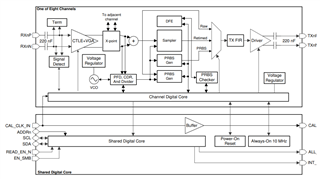
2: how is the crosspoint of DS250DF810 ,please supply a pciture

3: the apply is 100G over 4 lane in zqsfp+,please supply eeporm file.

4: the designe use two the chips,the pin cal_clk_in use the crystal separately, the pin cal_clk_out (E15) is noconnection,is this ok?

5:what is the price and how to buy it in beijing of china

    1. Please see the "SMBus Master Mode" section of the data sheet and the pin descriptions for ENSMB and READ_EN_N.
      • EN_SMB -> Float
      • READ_EN_N -> Pull down
        • If you're using the same EEPROM for two devices, set READ_EN_N -> pull down on device 1.  For device 2, cascade ALL_DONE_N from device 1 to READ_EN_N of device 2.
    2. I don't understand your question.  Can you please clarify?  Please see the block diagram and section on "Cross-Point Switch".
    3. Please note that I have configured this to device address 0x30, using adapt mode 2.  I'd encourage you to download SigCon Architect and the DS250DF810 profile.  This will allow you to generate your own EEPROM file.  Please also leave at least 3 dB of insertion loss between the DS250DF810 RX and any signal source. The DS250DF810 CTLE has a high minimum boost.  This will help reduce risk of over equalization.
      • https://e2e.ti.com/cfs-file/__key/communityserver-discussions-components-files/138/ds250df810_2D00_0x30_2D00_adapt_5F00_mode_5F00_2.hex
    4. Yes, it is okay to leave CAL_CLK_OUT as no-connect.
    5. I've reached out to a member of our sales team regarding price and purchasing in Beijing.  They may reach out to you in the next couple days.

    Thanks,

    Drew

  • Where is the chip in pcb ? is it near to the controller(cpu) or the connector (zqsfp+)? how to deal with the quesiton

  • 1:After eeprom is loaded, The leve of the pin all_done_n(D3) is low ?

    2: what is the capacity of eeprom at least?

  • the application use two the chips, output two zqsfp+ connect, the input clock of the two chips is from a source

  • Hi,

    Where is the chip in pcb ? is it near to the controller(cpu) or the connector (zqsfp+)? how to deal with the quesiton

    We often see the retimer placed closer to the connector.  However, this will depend on how much insertion loss is between the CPU <-> Connector and what sort of equalization capability the CPU has.  It's important that the insertion loss between CPU <-> Retimer is within the equalization capability of the CPU.

    Also, the retimer has a high boost at CTLE index 0.  Because of this, please leave at least 3 dB between the CPU <-> retimer and Connector <-> (assuming you will use optical modules).  This will help avoid over-equalization.

    1:After eeprom is loaded, The leve of the pin all_done_n(D3) is low ?

    Yes, this is correct.

    2: what is the capacity of eeprom at least?

    I'd recommend using either 1kByte or 2kByte EEPROM.

    Thanks,

    Drew