Part Number: DP83822H
Tool/software:
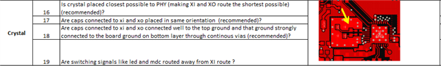
There is a recommendation for Crystal layout on competition MCU d/s as below layer 1/2/3. It looks there is a independent ground under Xstal.
We found a article below for layout suggestion. but there is no layout diagram to show how to do it. Is there detailed crystal layout suggestion with DP83822HRHBR? thanks.

Regards
Brian