This thread has been locked.

If you have a related question, please click the "Ask a related question" button in the top right corner. The newly created question will be automatically linked to this question.

NS16C2752: Unable to write to registers.

Part Number: NS16C2752

Tool/software:

I am Japanese. I am writing this thread using a translation application.

Hello TI Support Team.

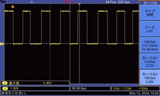
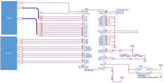
I am using NS16C2752, I cannot rewrite the internal registers.
Is there any operation that needs to be performed before writing the register or can the register be in a write disabled state?

  • Are you able to verify the logic levels on the input pins (address pins, CHSL, #WR, RD, ect) are toggling correctly?

    Can you also verify the MR is set properly and toggled at power up? 

    Can you write to LCR (address 3) and read back the written value to verify if the write properly went through? 

    Some registers require you to set certain bits within other registers inorder to write to them. We probably need to verify first if you can write to a register that doesn't have these conditions like LCR. 

    -Bobby

  • Thanks for the reply Bobby.

    I checked again and there was no problem with input pins or MR.

    I was also able to write to LCR and SCR without any write restrictions without any problems.

    But I cannot write to DLL and DLM registers.
    The procedure is as follows
    LCR=0x80
    DLL=0x02
    DLM=0x00
    LCR=0x03
    Writing is done in this order.

    The registers before rewriting the DLL and DLM registers have the following values.
    (adr)0x00,0x01,0x02,0x03,0x04,0x05,0x06,0x07
    (val)0x35,0x00,0x00,0x80,0x00,0x60,0xF0,0xFF

    Since LCR(0x3) is 0x80, I think it is possible to write to DLL and DLM, but do I need to set other registers?

  • Since LCR(0x3) is 0x80, I think it is possible to write to DLL and DLM, but do I need to set other registers?

    You shouldn't need to set the other registers. The only requirement to write to DLL/DLM is to write to LCR bit 7 set to '1' (LCR=0x80 and The total register cannot be 0xBF). 

    I might have a guess as to why you think you're not writing to these registers. 

    If you change the LCR register to 0x80 then write to DLL/DLM, you should immediately read both DLL/DLM BEFORE you change LCR to 0x03. If you try to read DLL/DLM after LCR is set to 0x03, then you won't be able to read DLL/DLM. You will end up reading the RBR/IER instead. 

    Are you verifying the DLL/DLM registers immediately after you write to them?

    Step 1: Write LCR =0x80

    Step 2: Write DLL = 0x02

    Step 3: read DLL

    Step 4: Write DLM = 0x00

    Step 5: read DLM

    Step 6: Write LCR = 0x03

    -Bobby

  • Are you verifying the DLL/DLM registers immediately after you write to them?
    Yes, read before LCR=0x03.

    Other overall register changes are made according to the following procedure.
    IER=0x01
    LCR=0x80
    DLM=0x00
    READ DLM
    DLL=0x02
    READ DLL
    LCR=0x03
    FCR=0x01
    FCR=0x07
    FCR=0x07
    We have performed this procedure and confirmed that all but DLL/DLM have been changed.

    For example, is it possible to write a register and then need some time for the value to be reflected?

    I have also included the register value when LCR[7]=0 just in case.
    (adr)0x00,0x01,0x02,0x03,0x04,0x05,0x06,0x07
    (val)0x00,0x01,0xC1,0x03,0x00,0x60,0xF0,0xFF

  • For example, is it possible to write a register and then need some time for the value to be reflected?

    There should be a slight delay but it shouldn't be something that you would need to wait a second or two to see. Seeing as you're able to read the other registers, its probably not related to a time delay. 

    Are you able to write to the AFR register and set the BAUDOUT bit? (AFRb1=1)

    Then probe the MF1/MF2 pins. If you write to the DLL/DLM registers you should see the Baudout pin change to become 16x of the baudrate. We can try to use this to verify if the registers are being written to (incase we can't read them correctly).

    Are you also able to share your schematic for the NS16C2752? 

    -Bobby

  • >Are you able to write to the AFR register and set the BAUDOUT bit? (AFRb1=1)
    >Then probe the MF1/MF2 pins.
    step1:AFR=0x02
    step2:READ DLL/DLM
    step3:DLM=0x00
    step4:DLL=0x02
    step5:READ DLL/DLM
    Comparing after step 1 and after step 4, there was no change in the output of MF2.
    The DLL/DLM values obtained in steps 2 and 5 are DLL=0xDE and DLM=0x01.
    The output of MF2 was captured and is attached.

    >Are you also able to share your schematic for the NS16C2752?
    Attached is a schematic diagram of the NS16C2752 peripheral.
    Please point out any incorrect connections.
    Read/write is executed from CPU1 and interrupt monitoring is executed from CPU2.

  • I don't see any big concerns with the schematic and it seems like you have local decoupling on Vcc.

    step1:AFR=0x02
    step2:READ DLL/DLM
    step3:DLM=0x00
    step4:DLL=0x02
    step5:READ DLL/DLM
    Comparing after step 1 and after step 4, there was no change in the output of MF2.
    The DLL/DLM values obtained in steps 2 and 5 are DLL=0xDE and DLM=0x01.

    Thanks for checking this. It seems that there are values in the registers but the steps provided aren't toggling them at all. The only other thing I can think of is to probe all the input pins during each step to verify the pins are actually set to what we expect. Maybe the other issue is the MR pin is somehow getting reset before we try to write to DLL/DLM... 

    Step 1: Write LCR =0x80

    Step 2: Write DLL = 0x02

    Step 3: read DLL

    Step 4: Write DLM = 0x00

    Step 5: read DLM

    Step 6: Write LCR = 0x03

    Can you add a step after 1 to read LCR to verify it's actually set properly?

    I think it may be a good idea to probe the address pins, CHsel, CS, RD, WR and the data lines when you write to LCR and DLL and then repeat for the read as well. 

    I would also monitor the MR pin to ensure it doesn't toggle during these steps. 

    -Bobby

  • Thanks for the answer Bobby.

    It looks like some other device was affecting the MR and was causing a HIGH input to the MR.
    I fixed it and checked and DLL and DLM were able to write without any problem.
    Thanks for your kind response so far.

    I'm still having trouble getting the data transmission to work, so I'll look at the datasheet and contact you again if I find anything I don't understand.
    Thank you for your response.

  • Glad you were able to find out the root cause of the DLL/DLM issue. 

    Feel free to create another e2e post if you aren't able to get the transmission working. 

    -Bobby