This thread has been locked.

If you have a related question, please click the "Ask a related question" button in the top right corner. The newly created question will be automatically linked to this question.

TRS3221E: Ripple Noise on V+ pin

Part Number: TRS3221E

Tool/software:

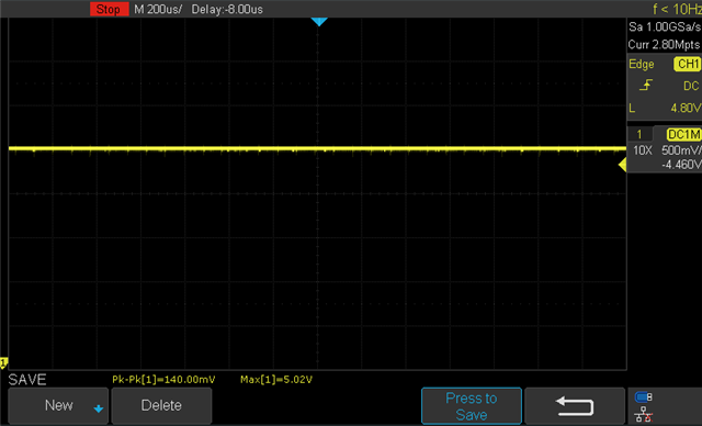
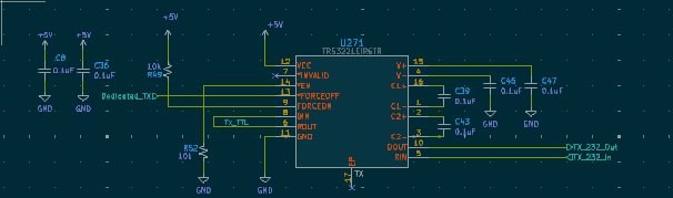
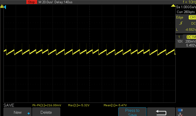
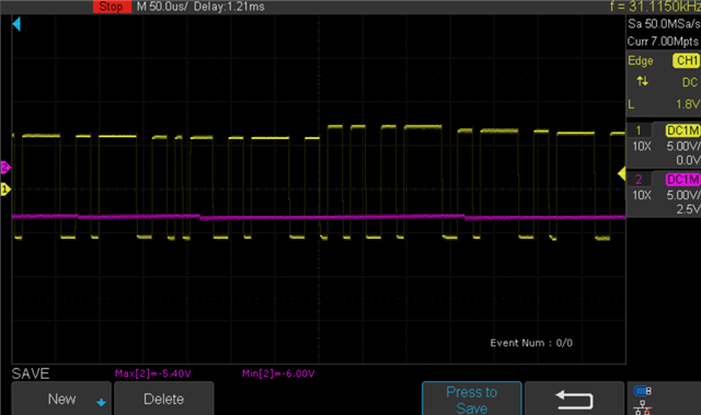
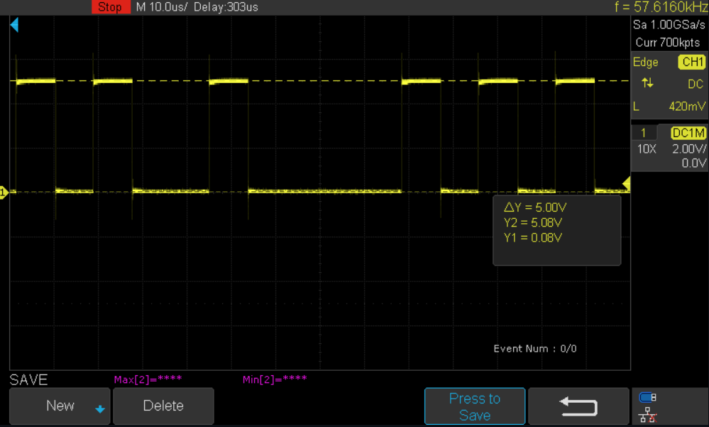
I am using the TRS3221EIRGTR RS-232 transceiver in my design and am noticing significant ripple noise on the V+ rail. The supply voltage is 5V, and I have placed a 0.2µF bypass capacitor between Vcc and ground. Initially, I used 0.1µF capacitors for the charge pump, and with this setup, I observed a ripple voltage of approximately 1.5V on the V+ rail. The capacitors are placed on the bottom of the PCB, right next to the pins of the transceiver, so I do not believe it is a layout issue. When observing an RS-232 signal at the DOUT pin with a load connected, the waveform shows a sawtooth pattern when the signal is high.

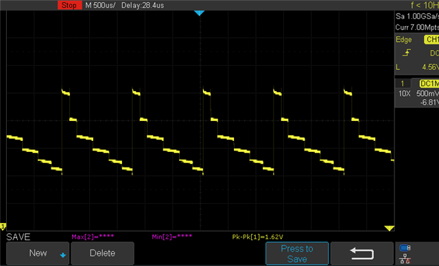
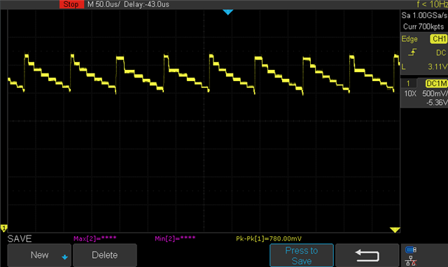
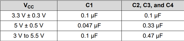
I reviewed the charge pump functionality in the application note, How the RS-232 transceiver’s regulated charge-pump circuitry works, and based on Equation 2 from the document, I attempted to reduce the ripple by adjusting the capacitor values. I changed the capacitor values C1 = 0.1µF and C2, C3, C4 = 0.4µF, which reduced the ripple to approximately 500mV. I also tried increasing the values to C1 = 0.1µF and C2, C3, C4 = 1µF, as suggested by the waveforms in the document, but the ripple voltage increased to approximately 650mV.

Are there any additional recommendations or techniques for further reducing the ripple on the V+ rail? Any insights would be greatly appreciated.

  • 1.5 V is too high.

    What is the average V+ voltage? What is the output load? Is it possible that there is a short somewhere?

  • Hi Matt,

    Could you please share your layout and schematic? Just a PDF or image of the charge pump areas would be ideal. 

    For the best functionality, the capacitor values found in the datasheet should always be used. Otherwise capacitors outside the suggested values will introduce more problems than it can solve. 

    If the suggested values are used, you do not need to worry about the full charge pump functionality and voltage levels. Unless there is a more critical problem like Clemens is suggesting. 

    Best,

    Ethan

  • Hi Clemens and Ethan,

    There no short on the 5V rail. Below is a screenshot showing the 5V rail across the bypass capacitor.

    Additionally, here is a screenshot of the ripple observed on the pin V+. In this measurement, C1,C2,C3, and C4 are all 0.1uF, and the ripple is approximately 1.5V.

    To reduce the ripple, I adjusted the capacitor values:  C1 remains at 0.1uF, while C2,C3, and C4 were increased to 0.4uF. With this adjustment, the ripple decreased to approximately 500mV.

    Here is my schematic. 


  • What is connected to the DOUT pin?

    Does the V− voltage look OK?

    What are the absolute average values of V+ and V−?

  • The DOUT pin is connected to the RX pin of a USB-to-RS232 cable. I have a terminal open on my computer (terra term), and I am successfully receiving data transmitted from the DOUT pin of the transceiver to the cable. I also tested the USB-to-RS232 cable with other RS-232 equipment, and the TX/RX signals did not exhibit the inconsistent peak-to-peak output observed in the waveform I attached earlier.

    Below is a screen capture showing the V− rail, measured across capacitor C4, which is located directly beneath the V− pin of the transceiver.

    The average voltage of the V+ rail is 6.35V, and the average voltage of the V− rail is 5.47V.

  • I realized I forgot to attach the screenshot of the data at the DOUT pin in my earlier post.

    Here is the screenshot showing the data transmitted through the transceiver, measured at the DOUT pin.

    Here is the data at the DIN pin of the transceiver.  

  • Hi Matt,

    We only guarantee that the device will be fully functional with the capacitance values listed in the datasheet. However, you can attempt custom capacitor values at your own risk. The critical piece here is the ratio between C1 and C2,C3, C4. Rule of thumb is that there should be between a 10:1 to 5:1 ratio with the C1 being the smaller value, and no capacitors should be larger than 1uF. 

    For the DOUT image you recently posted, what capacitor values were used? If 0.1uF were used for C1-C4 with VCC at 5V, then it makes sense why the peak is higher using the formula in that charge pump article.

    Might I also ask why you are concerned with the voltage ripple if the device is communicating successfully?

    Regards,

    Ethan 

  • An RS-232 receiver has an impedance of about 5 kΩ.

    In the waveforms shown, the bus output is negative, so both V+ and V− are loaded. (V− is generated from V+.) The high-frequency ripple is the V− charge pump. The lower-frequency ripple is the V+ charge pump, and I do not know why it does not switch with a higher frequency.

    As far as I can see, you are not using the capacitor values recommended for a 5 V supply. Please check how the ripple looks with the correct values.

    The capacitor(s) at the VCC pin can be increased if you want to reduce the ripple on your 5 V supply.
    The capacitors at the V+ and V− pins can be increased to reduce the ripple on the output supplies, but then they will take longer to power up.
    You should not change the flying capacitors (C39, C43) from their recommended values/ratios. Increasing them will increase the ripple and lower the ripple frequency.

  • Thanks Ethan and Clemens,

    I initially used 0.1uF for the charge pump, but I observed that the ripple was much larger than expected. Following TI's recommendation from the app note and this document, I adjusted the capacitance. Specifically, I changed the capacitance so C39 = 0.1uF and C43, C45, and C47 = 0.5uF.

    Despite these changes, I'm still seeing a ripple of approximately 500mV. This also impacts the signal integrity at the DOUT pin (posted above). This is concerning because I have the same transceiver on a 3V3 rail that exhibits a much smaller ripple. Even after adjusting the capacitors for the transceiver on the 5V rail based on the app note, the ripple remains significantly larger than the ripple on the 3V3 rail.

    Is there anything further I can try to reduce the ripple? It would be helpful to know the expected ripple when using the capacitors recommended in their app note.

     Thank you.

  • Matt,

    I re-read your first post, and I realized you placed the caps on the bottom layer. Doing this means you have vias that introduce inductance which is not ideal. The charge pump caps should always be on the top layer and as close to the pins as possible. Otherwise, I still recommend changing C1-C4 to match the 5V specific configuration to minimize the ripple if you are still seeing it affect DOUT. 

    Regards,

    Ethan