This thread has been locked.

If you have a related question, please click the "Ask a related question" button in the top right corner. The newly created question will be automatically linked to this question.

TCAN1042-Q1: CAN Termination control using GPIO

Part Number: TCAN1042-Q1
Other Parts Discussed in Thread: ESD2CAN24, CSD, CSD17483F4, CSD87502Q2

Tool/software:

Hi Team,

My application includes a CAN interface, which requires GPIO control for enabling and disabling the 120ohm CAN termination.

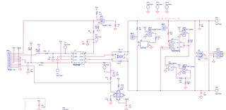
Referred to the TI Implementation shared below for this

can selectable termination.opj

Taking this as a reference, implemented the CAN termination control using GPIO as shown below

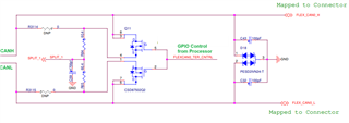
Could you please review this implementation and share your feedback? 

  • Hi Sandra,

    I do not believe the the CSD devices are biased correctly for the needed 120 ohms as Gate and Drain seems to be shorted together and have moved the thread to the HVP-FET team to help double confirm. Furthermore, please help promote TI's ESD2CAN24 for CAN applications, thanks.

    Best Regards,

    Michael.

  • 1. As Michael said, in this implementation, the termination resistors are always disconnected on one side. It would be enough to (dis)connect them with a switch on one side.

    2. There are CAN bus applications where there can be a large ground offset between nodes. In that case, the range of bus voltages make it impossible to bias the MOSFET gate(s) with just a GPIO signal. What are the bus voltages that can actually happen in your application?

  • Hi Sandra,

    I'm not very familiar with this type of application. Looking at the TI reference design documentation, the CSD87502Q2 FET gates are pulled up to VCC thru a resistor and pulled down by the CSD17483F4. Assuming VCC = 5V and the signal at each drain switches between 0V and 1V, VGS will vary from about 4V up to 5V which should be adequate as the CSD87502Q2 has Rds(on) specified down to VGS = 3.8V in the datasheet. If you are trying to drive the CSD87502Q2 gates directly from a GPIO signal then the high level needs to be ~5V. Otherwise, you will have to implement a drive scheme similar to the TI reference design. The gate of the CSD17483F4 can be driven directly by the GPIO signal as long has the high level is at least 1.8V. The CSD17483F4 acts as an inverter which needs to be taken into account. Please let me know if you have any quesitons.

    Best Regards,

    John Wallace

    TI FET Applications

  • Hi Sandra,

    Following up to see if your issue has been resolved. Please let me know.

    Thanks,

    John

  • Hi Sandra,

    Since I have not gotten a response, I assume your issue is resolved and will close this thread.

    Thanks,

    John

  • Thanks, John, Clemens & Michael for sharing the detailed review comments.

    We did a simulation using the CSD87502Q2 Mosfet, and it was not turning on fully using the 3.3V level. We updated the voltage level of the signal controlling the gate of the Mosfet, and now it is turning on as expected in the simulation.

    Thanks for the support Team!

  • FYI the CSD87502Q2 needs VGS ≥ 3.8V to be fully on. That is the minimum value of VGS where Rds(on) is specified in the datasheet and tested in production. With VGS < 3.8V, Rds(on) is not guaranteed.