This thread has been locked.

If you have a related question, please click the "Ask a related question" button in the top right corner. The newly created question will be automatically linked to this question.

DP83848C: Layout question

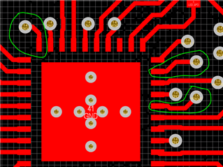
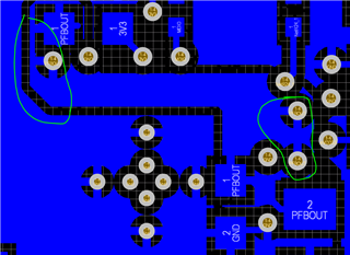
Part Number: DP83848C

Tool/software:

Dear Sirs , 

I am working on a layout with DP83848C and I am wondering if the PFBOUT 23 can be connected with a wire under the IC with pin 18 and 37 . 

I have a bit a space constraint design and if I can rout them under the ic that would help 

  • Hi Gerwin,

    Thanks for submitting your query, I would be glad to help. Yes you can! For reference, please refer to the DP83848K-MAU-EK. The Altium layout file is available in the Design Files tab.

    Note that this is the 848K variant of the part, the PFBOUT pins are 19, 16, & 31, instead of 23, 18, & 37 for the C variant.

    The pins go through a VIA from the Top Layer to the Bottom (GND) layer, where they are all connected.

    Figure 1- 848K EVM Top layer Layout

    Top Layer

    Bottom Layer

    Regards,

    Alvaro

  • Hi Alvaro , 

    I made this out of it : 

    I am using a 6 layer board due to some other things I need to add , for RMII signal length matching I have some issue with TXD0 -TXD1 (approx 47mm) and RXD approx 37mm the ref_clock is 37mm , I routed the signals on top and bottom and some low speed signal on layer 4 , do you think the length difference with TXD and RXd really matters ? I read somewhere that the difference can be 12mm (RXD0 and RXD1 are matched , like TXD0 and TXD1)

  • Hi Gerwin,

    Because both the TX and RX data pins operate off the same RMII Clock, this could cause communication issues. If it were MII or RGMII, where both the TXD and RXD have their own respective TX/RX clock, I would agree with your current layout.

    General rule of thumb would be to keep the data lines within 100mils length match with respect to the clock.

    Regards,

    Alvaro