Part Number: TCA9517A
Tool/software:
Hi team
My client has some questions about how the datasheet specifications should be viewed.
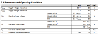
1. The customer said that VIL VIH VOL VOH these parameters have a maximum value and a minimum value or an intermediate value. Which one should be compared to be correct, or should it be within this range? In addition, why do some have only maximum values and no minimum values?
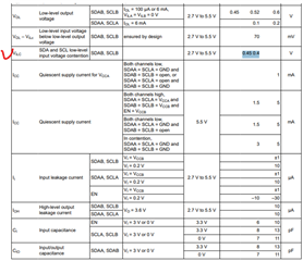
2. Can you also help explain what VLC is?
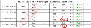
3. And why does VLC have 0.45 and 0.4, which value should customers look at?
Thanks,
Boyan