This thread has been locked.

If you have a related question, please click the "Ask a related question" button in the top right corner. The newly created question will be automatically linked to this question.

TPD4S311A: Consultation on TPD4S311AYBFR usage issues

Part Number: TPD4S311A

Tool/software:

Hi Teams,

The customer found a problem while using the TPD4S311AYBFR . Please help confirm and reply. Thank you!

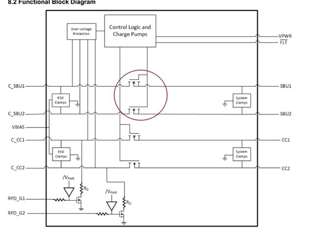
The connection diagram is as follows. As the customer did not use the SBU signal on the Type-C connector, after confirmation with TI engineers, it can be used to protect the D+/- signal of USB2.0 with C_SBU1/2:

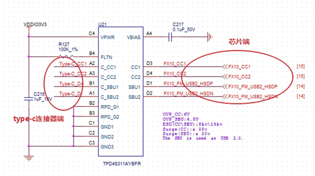
The current problem caused by this usage is that on the ASMedia USB 3.1 interface that comes with the host motherboard model (Prime H270-PRO), the device cannot be stably connected using the USB2.0 D+/- signal, and there are occasional issues.

Question:
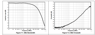
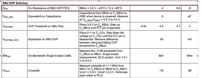
1. Could you please help confirm again whether the C_SBU1/2 pin of TPD4S311AYBFR can be used for protecting USB 2.0 signals?
2. If it can be used in this way, how can we solve the problem of unstable connection we encounter?

  • Hi VAyne,

    The Datasheet shows that the SBU pins of the device have 1Ghz of Bandwidth (Based on the insertion loss figure) and about 45dB of crosstalk immunity at 500Mhz.

    Based on these values, it is possible to use these pins for USB2.0 signals as long as there are not other switches in the datapath.

    Regards,

    Chuck

  • Hi Chuck

    Thank you for your reply,

    Does the conduction impedance of the SBU channel refer to the conduction impedance of the MOSFET shown in the chip diagram? If its conduction impedance reaches 4~6.5 Ω, will it cause significant signal amplitude attenuation? Is channel insertion loss related to signal type? Is it possible that this channel has a smaller insertion loss when using SBU type signals, while there may be issues when using USB2.0 signals?

  • Hi Vayne,

    Yes, the impedance shown is the resistance of the SBU path.  This resistance along with the capacitance of the ESD structures and package are what limits the bandwidth of the switch.

    That is shown in the figure that I showed above.  A channel that has 1Ghz of bandwidth like the SBU path will be able to pass USB2.0 signals without significant degradation.

    Regards,

    Chuck