


Part Number: TVS2701
Tool/software:
These days I'm in an external laboratory to do the EMC and RED tests on our new industrial gateway to release the CE certify and I need to close the activity in the next few days.
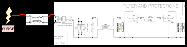
I put below the schema and the lay-out of the first stage of power line input:
I tested BURST on power line with no problems (fast transients common mode - ETSI EN 301 489-1, Par 9.4 - EN 61000-4-4 500V)
I had a problem in the SURGE on power line test, after the 3rd discharge.
The surge tests are at 0.5KV: ETSI EN 301 489-1, Par 9.8 / EN 61000-4-5 ( ±0.5kV(1kV) all lines to Ground(1,2/50 μs)(42 Ohm)).
In the first stage of the power line input I have a TVS2701DRBR. I selected this component because of the very small interval from the gateway Vin max and the absolute maximum input voltage of the first DC/DC stage:
- Vin MAX (gateway) = 28,8Vdc
- Vin DC/DC MAX = 34V (above this value the DC/DC can be damaged).
The external common mode choke was added to kill noise from the gateway to the power line, like I saw during the EMC tests.
In the final PCB the choke will be inserted in place of the current F45 (see the drawing above).
For sure I had a mistake using this lay-out for surge because the TVS is after the choke, so the filter is exposed to all the surge. In the next tests I'll try to insert it in the right position (F45) even if "on the fly".
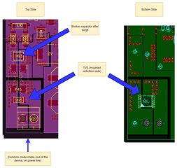
After the test I saw these damages:
- External choke:
- Positive winding open.
- Negative winding seem ok.
- TVS2701DRBR is not in short circuit, but I can't test if it's ok or if it's broken (open).
- C193 is obtained by 2 multilayer ceramic capacitors (1210 10uF50V X5R) mounted in parallel (physically one on the other). One of these is shorted after surge tests (I can see a fracture in the ceramic body).
About this problem I have some questions:
- Is TVS2701DRBR the correct choice in this context?
- Can I say that the problem would be caused all by the external common mode filter or I must to expect to have the same problem with the filter inside after the TVS?
- Is the design scheme correct or do you see some critical points?
- If necessary an hw modification the ideal is to be able to make it on the fly and in a second time to modify the PCB, so to end the whole tests.
Thank you in advance for your time.
