This thread has been locked.

If you have a related question, please click the "Ask a related question" button in the top right corner. The newly created question will be automatically linked to this question.

SN65MLVD204: Wired-OR Signaling Using M-LVDS Drivers and Receivers

Part Number: SN65MLVD204

Tool/software:

Hi team,

There are questions about the wired-of sinaling described in the app note, that is Wired-Logic Signaling With M-LVDS.

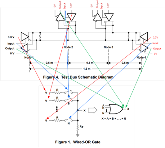
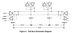
1. In the figure 4, is it no problem to make input pins of multiple devices High at the same time? Can this lead to device destruction?
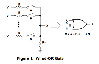
2. Input pins in figure 4 can be equivalent to switches A~N in figure 1. Is this understanding correct?
Regards,

Noriyuki Takahashi

  • An LVDS transmitter has three outputs states, high (Y > Z), low (Y < Z), and idle; the idle state is controlled with DE. On a normal half-duplex bus, no more than one transmitter should be active at the same time. If multiple transmitters are active and output different values, then the differential voltage on the bus is likely to be invalid.

    The app note describes a mechanism to implent wired-OR signalling; this is done by using only two states, high and idle. (Please note that the logic input signal goes to the DE pin.) When multiple transmitters output a high signal, the differential bus voltage still is valid.

    Figure 1 is just an explanation, and does not correspond to the actual circuit.

  • Hello,

    There can be issues when a device on a bus wants to drive a signal high, while another is driving low. This is called bus contention. If these devices send and receive data at the same time, a short circuit may occur if one is driving high to logic '1' (say to the supply voltage) and the other is driving low to logic '0' (say to ground). In the case of a short circuit, devices typically having ratings listed in the datasheet. The Wired-Or method provides the equivalent of OR gating all of the outputs to a signal line and collision detection.

    Thank you,

    Amy

  • Amy

    Here are additonal questions.

    As below figure, I assume that figure 1 can be compatible with figure 4 as below picutre.

    In term of this assumption, do you think that Clemens's comment as belwo is correct? If it is correct, can this operation lead to device destruction?

    The app note describes a mechanism to implent wired-OR signalling; this is done by using only two states, high and idle. (Please note that the logic input signal goes to the DE pin.) When multiple transmitters output a high signal, the differential bus voltage still is valid.

    Regards,

    Noriyuki Takahashi

  • Hi Noriyuki-san,

    Thank you for the drawing. The wired-OR gate ensures that contention does not occur. I do agree with Clemens in that this results in only two state options, as the "OR" function eliminates a short circuit condition possibility, thus making the differential bus voltage valid at all times with no concern of device damage.

    Thank you, Amy