This thread has been locked.

If you have a related question, please click the "Ask a related question" button in the top right corner. The newly created question will be automatically linked to this question.

AM26C31: High level Output voltage (VOH)

Part Number: AM26C31
Other Parts Discussed in Thread: AM26LV31

Tool/software:

Hi TI Team,

1. Why this IC (AM26C31QDR) Voh value provided in datasheet?

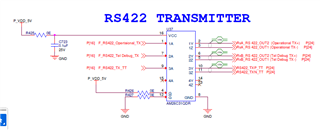
2. AM26C31Q input pin's connected to 3V3 volt FPGA bank so could please review below mentioned table and confirm should we use level shifter or not for this IC?

                           FPGA (XQZU19EG-2FFQB1517I) - RS422 RECIEVER (ACPL-064L-560E)                             Margin
FPGA (XQZU19EG-2FFQB1517I) RS422 RECIEVER (ACPL-064L-560E) FPGA DRIVING RS422 RECIEVER DRIVING
Voh(min) (V)  Vol(max) (V) Vih(min) (V) Vil(max) (V) Voh(min) (V) Vol(max) (V) Vih(min) (V) Vil(max) (V) Voh-Vih Vil-Vol Voh-Vih Vil-Vol
2.9 0.4 2 0.8 2.3 0.4 2.9 -0.4 0.3 0.4

Thanks for considering my request !.

  • Is this the correct table? It does not mention the AM26C31 but a receiver.

    Please note that VOL/VOH values are specified for a certain test current; with an input current of a few µA, the actual output voltages will be near VCC/GND.

    The AM26C31's inputs are designed to be TTL compatible (VIH = 2 V), so it is possible to input 3.3 V signals. (Alternatively, you could use the AM26LV31(E) with a 3.3 V supply.)

  • Hi Clemens Ladisch,

    Thanks for the support !

    Please review I/O voltage level analysis table for AM26C31QDR and confirm whether level shifter is required or not. sorry for mentioned wrong data.

    FPGA (XQZU19EG-2FFQB1517I) - RS422 TRANSMITTER (AM26C31QDR) Margin
    FPGA (XQZU19EG-2FFQB1517I) RS422 TRANSMITTER (AM26C31QDR) FPGA DRIVING RS422 TRANSMITTER DRIVING
    Voh(min) (V)  Vol(max) (V) Vih(min) (V) Vil(max) (V) Voh(min) (V) Vol(max) (V) Vih(min) (V) Vil(max) (V) Voh-Vih Vil-Vol Voh-Vih Vil-Vol
    2.9 0.4 2 0.8 2.2 0.4 2 0.8 0.9 0.4 0.2 0.4
  • Hi Clemens

    Thanks for your response,

    Following is our schematics. We have interfaced the AM26C31 inputs to an FPGA bank operating at 3.3V. Please let us know if this is ok.

  • The input leakage current of the AM26C31 is at most 1 µA, so the FPGA's actual VOL and VOH values are near 0 V and 3.3 V; the margin us much larger. (For CMOS outputs connected to CMOS inputs, VOL/VOH calculations usually are not necessary.)

    There is no signal from the transmitter to the FPGA; the last two columns are meaningless.

    The 4A input must not be left floating; connect it to VCC or GND.

  • Hi,

    Clemens is correct. The A pins of the Am26C31 device are high impedance so the VoH/VoL of the FPGA to the A pins should pull close to Vcc/GND since A pin isn't a strong current source (your VoH and VoLs from the FPGA are likely rated for mAs of current but the A input is probably sub uA which is why they will push closer to GND/Vcc).

    The VoH/VoL specs from AM26LV31 don't mean anything to the FPGA if its interfacing on the a pin.

    Please also note that Clemens comment about not letting 4A float is correct as well. Tie this pin to Vcc or GND with a resistor to prevent shoot through current.

    -Bobby