This thread has been locked.

If you have a related question, please click the "Ask a related question" button in the top right corner. The newly created question will be automatically linked to this question.

DP83825I: About clock shift

Part Number: DP83825I


Tool/software:

Hi team,

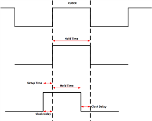
DP83825I did not recognize TX properly when operated as slave mode.
However, when I enabled RMII_TX_Clock_Shift, it worked fine.
I assume this is due to the fact that there was no hold or setup time provided for the TX, correct?
I also did not know which time is clock shifted when this register is enabled at this time.
Can you please tell me where to look in the datasheet?

Best Regards,
Ryu.

  • Hi Ryu,

    Given that the issue is fixed after enabling the clock shift, it does look like it was a sampling problem, not enough setup/hold time. 

    I took a look at the datasheet as well and there doesn't seem to be a value listed for the shift time. Let me confirm with my team if we have this data and respond back to you within the week. 

    Best,

    Vivaan

  • Hi Vivaan,

    How about progress on this one?

    Best Regards,
    Ryu.

  • Hi Ryu, 

    Due to the Holidays this time of the year, we are having some delays getting in contact with our design teams. I will have an answer for you by the end of next week. Thank you for your patience.

    Best,

    Vivaan

  • Hi Vivaan,

    Yes, I understand.
    I look forward to your response as soon as possible.

    Please tell us additional information.
    I found the following statement on p9 of the datasheet
    RMII Slave Output Timing default supports setup time upto 7.5 ns. For 7.5ns to 10.5ns, program register 0x0017.8 = 1, 0x0042=0x0014”
    However, this register is not found.
    Can you also give me the details that this statement means?

    Best Regards,
    Ryu.

  • Hi Ryu,

    Yes, I understand.
    I look forward to your response as soon as possible.

    Thank you for your understanding. 

    However, this register is not found

    The register 0x0017 can be found in the datasheet register map, but the register 0x0042 is a reserved register for internal testing use, which is why it is not a part of the public datasheet. However, we realized that one feature of this register was helpful in margin cases relating to RMII timing, which is why that note was added. If you face this marginal case, this register can be written to and used even though it is not a part of the datasheet register map

    Best,

    Vivaan

  • Hi Vivaan,

    I understood about registers.
    Did you understand the values?

    Best Regards,
    Ryu.

  • Hi Ryu, 

    I have spoken with our design team and am waiting for them to check the books and get back to me with the delay information. I will provide you this information as soon as it gets on my desk. Again, I apologize about the delays in communication a lot of people are out on holidays. 

    Best,

    Vivaan

  • Hi Vivaan,

    Have you obtained the values?
    If not yet, I would like to know when it is likely to be available.

    Best Regards,
    Ryu.

  • Hi Ryu, 

    I just heard back from the design team. The delay should be a 4ns delay based on 0x17[8]

    Best,

    Vivaan

  • Hi Vivaan,

    Thanks for letting me know.
    Please tell me one more thing.
    Does this device have a maximum setup time of 7.5ns?
    If the clock shift is shifted by 4ns, does the original signal need to be 3ns or less?
    Please tell me more about this statement.
    “RMII Slave Output Timing default supports setup time upto 7.5 ns. For 7.5ns to 10.5ns, program register 0x0017.8 = 1, 0x0042=0x0014 ”

    Best Regards,
    Ryu.

  • Hello,

    Vivaan is OoO and will be expected to respond to your query at worst beginning of next week.

    Sincerely,

    Gerome

  • Hi Ryu, 

    The setup time refers to the time for which valid data is present on the signal before the rising edge of the clock. It does not effect the length of the original signal. 

    This statement says that if the expected setup time for RMII TX in Slave mode is between 7.5ns and 10.5ns, you would need to use the respective register writes. 

    Best,

    Vivaan

  • Hi Vivaan,

    I am not quite understanding this, so let me get it straight.
    I believe that 4ns is the minimum setup time required.
    If 4ns is not available, I thought that by shifting the clock, 4ns can be ensured and the problem will not occur.
    What do you mean by a maximum of 7.5ns?
    Is this the value with clock shifting?
    If it is still not enough (7.5ns~10.5ns), does it mean that the register can be adjusted to work?
    If possible, it would be easier to understand if you could show this in a diagram.

    Best Regards,
    Ryu.

  • Hi Ryu, 

    Yes, 4ns is the minimum setup time required. 

    However, the maximum setup time supported is 7.5ns.

    This means that if the measured time delay on the pins falls between 7.5ns and 10.5ns, you would need to do the following register writes. (program register 0x0017.8 = 1, 0x0042=0x0014)

    This is not taking into account the clock shifting of register 0x17. The clock shifting enabled though this register happens internally, therefore, its effects cannot be measured on the pin itself. This is talking about the time delay measured on the pin. The delay measured on the pin can be due to trace delays or an internal delay added from the SoC side. Whatever the case may be, this delay is the one being referred to, not the internal PHY delay. 

    I hope this makes it more clear. 

    Best,

    Vivaan

  • Hi Vivaan,

    Sorry.
    I still don't understand.
    I think that if the delay measured at the pin is 7.5ns to 10.5ns, then shifting 4ns internally by clock shift will not reach the minimum of 4ns and will not be recognized.
    What timing are we talking about when the original data can be set up for how much setup time?
    For example, if the data is transmitted with no delay at all and a setup time of 4ns is secured, I would expect a setup time of 8ns when the clock is shifted.
    If this data is delayed by 7.5ns, the setup time will be only 0.5ns even if the clock is shifted.
    Is my understanding wrong?

    Best Regards,
    Ryu.

  • Hi Ryu, 

    There are 3 situations we are looking at in this application

    1. There is no SoC delay or trace delay on TX. The data and clock come in at the exact same time. In this case, the minimum requirement of 4ns setup time is not met since the rising edge of the clock is in phase with the data. In this case, we would need to enable the internal delay on the PHY side using register 0x17
    2. There is a small amount of delay being added (above 4ns and under 7.5ns) on the clock due to trace OR SoC. In this case, we do not need to enable the internal delay at all since the setup requirement is already met by the clock being delayed
    3. There is a larger amount of delay being added (above 7.5ns and under 10.5ns) on the clock due to trace OR SoC. In this case, we must do the following register writes (program register 0x0017.8 = 1, 0x0042=0x0014). This is a special edge case that we have noticed which requires these register writes to be done to function properly. 
    I think that if the delay measured at the pin is 7.5ns to 10.5ns, then shifting 4ns internally by clock shift will not reach the minimum of 4ns and will not be recognized.

    As you mention, since the delay measured at the pin is 7.5ns to 10.5ns, it is already meeting the minimum of 4ns since 7.5ns > 4ns. These register writes are simply a workaround we have found to make the device function normally in this edge case. Do not think of these register writes in terms of delays. 

    For example, if the data is transmitted with no delay at all and a setup time of 4ns is secured, I would expect a setup time of 8ns when the clock is shifted.

    If the data was transmitted with no delay, the setup time would be 0ns, and therefore cannot secure the 4ns requirement. Adding the internal delay would cause it to shift by 4ns, which would then mean a total delay/setup time of 4ns which meets the requirement, not 8ns. 

    If this data is delayed by 7.5ns, the setup time will be only 0.5ns even if the clock is shifted

    I don't think the data is being delayed at all. The delays are measured in terms of the delay between the data and the clock. The clock is the one that should be delayed by 7.5ns, which would yield a setup time of 7.5ns.

    Best,

    Vivaan

  • Hi Ryu, 

    I made the following diagram to exemplify the setup/hold times. 

    The middle data signal is one without a clock shift. We can see that since the rising edges are aligned to the clock signal above. Because of this alignment, we can see that there is no setup time. 

    The bottom data signal is shifted to the left to exemplify a clock delay. This is the same thing as delaying the clock to the right. In this case, we can see that there is a small setup time, which is equal to the clock delay being added. This is why if there is a delay of 4ns, the setup time would be 4ns.

    Does this make it a bit more clear?

    Best,

    Vivaan

  • Hi Vivaan,

    Thank you very much.
    I understood about the content.
    However, as shown in the figure below, there is a delay of up to 13ns in the data on my device, does this mean that DP83825I cannot be used on such a device?

    Best Regards,
    Ryu.

  • Hi Ryu, 

    I am not familiar with the MAC device this figure is representing since it is not a TI part, and therefore can't comment on its design.

    Regardless, as long as the timing requirement of the PHY is met, the device should perform as expected.

    best,

    Vivaan