This thread has been locked.

If you have a related question, please click the "Ask a related question" button in the top right corner. The newly created question will be automatically linked to this question.

P82B96: P82B96PWR

Part Number: P82B96
Other Parts Discussed in Thread: TCA9617B

Tool/software:

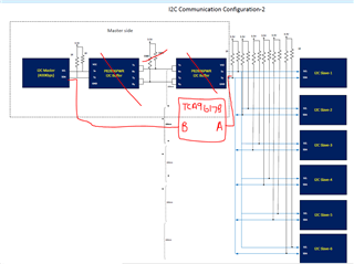
Master will communicate with 6 slaves through I2C buffer(P82B96PWR), each slave is at a distance of 100mm from the master, last slave is at a distance of 600mm. Master is in one PCBA and all slaves are interconnected through board to board connector .

1) Please suggest which configuration of BUFFER is works better?i2C Config-two options-for Ti Application Eng.pdf

2) Need P82B96PWR I2C buffer "pspice for Ti" or TINA simulation model to simulate the circuit.

  • Hi Kumarswamy,

    Reviewing the PDF file you attached, worst case longest trace is 700 mm = 70 cm. I usually estimate ~ 1pF / 1 cm which comes out to roughly 70 pF of trace. 

    The P82B96 was designed for long distance communication across a long cable. Stacking several P82B96 might be over designing for your system. P82B96 can buffer up to 4000 pF of cap load on the transmission side. 

    Just to clarify in the PDF, are there 3 configurations you are trying to decide between? This includes a series stacking of buffers vs. 2 parallel combinations? 

    As for PSPICE for the P82B96, we do not have this type of model, only IBIS model. 

    Regards,

    Tyler

  • Hi Tyler, 

    Thanks for quick response. The first block is application scenario, and we are thinking to use either of one Configuration. Could you please let us know which configuration best for our application. or suggest a NEW configuration with master is driving 6 slaves, each slave is at 100mm apart.

    Regards

    Kumar

  • And what is the next option to simulate the P82B96 ?

  • Hi Kumarswamy,

    P82B96 stacking in parallel configuration 1 seems like an over-design for the allotted capacitance. If there were longer cables of meters in length on each slave # segment, then it would make a little more sense to use several P82B96 in a parallel configuration. 

    In configuration 2, the long cabling should be between the pair of P82B96 devices. Is there 100 mm of distance between the pair of P82B96's? Is there still 100 mm separation between each slave on the Sx/Sy pins of the P82B96? 

    You might be able to solve this with only 1 buffer device. Let me know if the following design makes sense. 

    I assume that the distance between master and B-side of the TCA9617B is 100mm, and then the A-side longest stub length between A-side of TCA9617B and Slave 6 is 600 mm

    Regards,

    Tyler

  • Hi Tyler, Thanks.

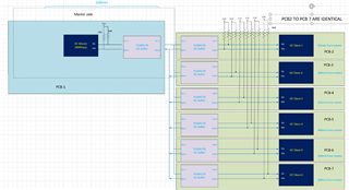
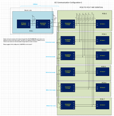
    Does Configuration-1 work for lower length also? Here is the actual application. All Slave PCBs are identical, and we are stacking up through connector.

    The distance between the master and first slave is 100mm, second slave is at 200mm, third slave is at 300mm and so on, please refer above snap.

    For Config-2: Since PCB2 to PCB7 are identical we need to have TCA9617B in all slave PCBs, so finally one buffer(TCA9617B) in master and one buffer will be in slave. refer below snap.

    With P82B96 also same interface , refer below snap

    Hope I clarified your points, look forward for your confirmation on the I2C buffer interface.

    Regards

    Kumar

  • Hi Kumar,

    Does Configuration-1 work for lower length also? Here is the actual application. All Slave PCBs are identical, and we are stacking up through connector.

    The distance between the master and first slave is 100mm, second slave is at 200mm, third slave is at 300mm and so on, please refer above snap.

    It can work, but things like trace cap, input cap, data rate, and PU resistors need to be accounted for. 

    Worst case would be if the host controller communicates I2C through each connector in series to the slave #6 in the chain, especially if there are buffer devices separating each PCB board. Each buffer adds prop delay. I have found that customers that chain multiple buffers in series usually have to lower their data rates because of the round-trip delay. 

    However, I also noticed that in configuration 1 the host controller can either communicate through the external bus wiring shown, or it can communicate through the connectors. Is this an intentional design? 

    For Config-2: Since PCB2 to PCB7 are identical we need to have TCA9617B in all slave PCBs, so finally one buffer(TCA9617B) in master and one buffer will be in slave. refer below snap.

    I like this configuration the most since I think it will be the best cost and simplest design. My only recommendation is that the TCA9617B on master side flips A and B sides. Connect the buffers in such a way so that A-to-A connection exists, not A-to-B. 

    The reasoning is that the static voltage offset should not face long inductive cable side. 

    Also, there needs to be PU resistors between the buffer-to-buffer connections on the cable side. 

    Another note is that you are using 240 ohm PU resistors on master side. Can the master sink ~12 mA of current? Otherwise, I would recommend weaker PU resistors maybe 2.7k to reduce current sink. 

    820 ohm on PCB-# is fine. 

    Hope I clarified your points, look forward for your confirmation on the I2C buffer interface.

    P82B96 parallel stacking seems over-designed. I think we can pass on this design and opt for the TCA9617B. P82B96 is more expensive than TCA9617B.

    Let me know your thoughts. 

    Regards,

    Tyler 

  • Thank you, we will go ahead with configuration-2(i.e TAC9617B on master and another buffer TAC9617B slave), and we will ensure that A-to-A connection exists, not A-to-B.

  • Hi Kumarswamy,

    B-to-A connection can exist, I would just recommend not having B-side face any long cabling. 

    Regards,

    Tyler